Design of a Primitive Nanofactory
Journal
of Evolution and Technology -
Vol. 13 - October
2003 -
 PDF Version PDF Version
http://jetpress.org/volume13/Nanofactory.htm
Chris Phoenix
Director of Research, Center for Responsible Nanotechnology http://CRNano.org
Abstract:
Molecular manufacturing requires more than mechanochemistry. A
single nanoscale fabricator cannot build macro-scale products. This
paper describes the mechanisms, structures, and processes of a prototypical
macro-scale, programmable nanofactory composed of many small fabricators.
Power requirements, control of mechanochemistry, reliability in the face
of radiation damage, convergent assembly processes and joint mechanisms,
and product design are discussed in detail, establishing that the design
should be capable of duplicating itself. Nanofactory parameters are
derived from plausible fabricator parameters. The pre-design of a
nanofactory and many products appears to be within today's capabilities.
Bootstrapping issues are discussed briefly, indicating that nanofactory
development might occur quite soon after fabricator development.
Given an assembler, a nanofactory appears feasible and worthwhile, and
should be accounted for in assembler policy discussions.
Contents:
1. Introduction
2. Background
2.1. Mechanochemistry
2.2. Mechanochemical fabricator
designs
2.3. Parts assembly, scaling,
and product integration
2.4. Nanofactory overview
3. Components and Innovations
3.1. A Thermodynamically Efficient
Stepping Drive
Figure 1:
Pin Drive
3.2. Joining Product Blocks
3.2.1.
The Expanding Ridge Joint
Figure
2: Expanding Ridge Joint
3.2.2.
Functional joints
4. Nanofactory Architecture
4.1. Mechanochemical functionality
Figure 3:
Workstation Grids
4.2. The reliable basic production
module
Figure 4:
Production Module
4.3. Gathering stages
Figure 5:
Convergent Assembly Fractal Stages
4.4. Casing and final assembly
stage
Figure 6:
Nanofactory Layout
4.5. Issues in bootstrapping
4.6. Improving the design
5. Product design
5.1. Levels of design
5.1.1.
Nanoparts
5.1.2.
Nanomachines
5.1.3.
Nanoblocks
5.1.4.
Patterns and Regions
5.1.5.
Folds
5.1.6.
Networks
5.2. Simulation and testing
5.2.1.
Design and simulation
5.2.2.
Testing and debugging a nanofactory-built product
6. Control of the nanofactory
6.1. Nanocomputer architecture
and requirements
6.2. Placing the nanoblocks
6.3. Specifying the nanoblocks
7. Product Performance
7.1. Strength, stiffness, and
shape
7.2. Appearance
7.3. Complexity
7.4. Design
7.5. Powering the product
7.6. Computation
8. Nanofactory calculations
8.1. File size and data distribution
8.2. Fabricator control, energy,
and cooling
8.3. Physical arrangement and
mass
8.4. Product cycle, duplication,
and bootstrapping time
8.5. Radiation and failure
8.6. Cost and difficulty of
manufacture
9. Conclusion and discussion
Appendix A. Calculations in software
Appendix B. Projections from the Merkle assembler
B.1. Mechanochemical baseline
B.2. Chemistry, electronics,
and mechanics
B.3. Mechanochemical error rate
References
1. Introduction
The utility of a new technology depends on many factors, including the
difficulty of development and the ease and cost of use. Most technologies
require significant additional work to form useful products. Previous
theoretical work in molecular nanotechnology has provided only incomplete
and fragmentary answers to the question of how molecular nanotechnologic
devices can be used in practice. Although it appears that fabrication
systems can be built on a nanometer scale (Drexler, 1992), small devices
will be difficult to use directly in many applications. Several designs
have been proposed in more or less detail (Drexler, 1986, 1992; Bishop,
1996; Merkle, 1997a; Hall, 1999; Freitas and Merkle, in press) for parallel
control of many small fabricators to make a large product. Other
proposals (Hall, 1993) combine many small products to create a large product.
However, each of these proposals has provided insufficient detail to allow
estimation of their practical difficulty and utility.
This paper builds on previous proposals to describe an architecture
for combining large numbers of programmable mechanochemical fabricators
into a manufacturing system, or nanofactory, capable of producing
a wide range of human-scale products. The proposed system is described
in sufficient detail to allow estimation of nanofactory mass, volume, power
requirements, reliability, fabrication time, and product capability and
cost, as simple functions of the properties of the mechanochemical fabricator
component. Bootstrapping a human-scale system from a sub-micron system
is also discussed. Discussion of product design issues and nanofactory
manufacturing capability demonstrates that the nanofactory should be able
to efficiently fabricate duplicates of itself as well as larger versions.
This proposal differs from previous proposals in that, with the exception
of mechanochemical component fabrication, design of the nanofactory should
be within the reach of present-day engineering; physical structures and
functional requirements are described in sufficient detail that remaining
problems should be within the capability of current engineering practice
to solve. In particular, the design considers all transport and manipulation
requirements for raw materials and product components, as well as control,
power, and cooling issues.
This exploration can provide a basis for estimating the practical value
and difficulty of developing a nanofactory. As noted in (Merkle,
1999), even a primitive sub-micron mechanochemical fabricator may produce
valuable products. The question at hand is whether, once such a device
is developed, it is feasible and worthwhile to adapt such devices into
a nanofactory. Since no complete designs, or even complete parameter
sets, exist for a mechanochemical fabricator, this question cannot be answered
fully at this time. However, the results of the present paper can
be applied to a wide range of hypothetical fabricator parameters.
As fabricator designs are proposed in increasing detail, these results
will become increasingly useful in predicting the capabilities of a nanofactory
based on such designs. Issues of product design and manufacture are
examined in order to establish that the nanofactory is capable of fabricating
duplicates and larger versions of itself. The time required to bootstrap
a human-scale factory from a nano-scale fabricator cannot be estimated
with any certainty, since bootstrapping will require time for debugging
and redesign as well as for fabrication of larger versions. However,
the minimum time required for fabrication can be estimated, and the design
developed here is simple enough that debugging and redesign may be fairly
simple and rapid.
The paper is arranged in several sections. Section 2
surveys previous work toward manufacturing systems relying on mechanochemistry
and producing human-scale products. Section 3 describes
two innovations required for efficient operation of the nanofactory architecture.
Section 4 describes the nanofactory architecture, including
a highly reliable
production module incorporating several thousand
mechanochemical fabricators and a scalable convergent assembly and transport
architecture for integrating large numbers of production modules.
Section 5 covers issues of product design to establish
that the nanofactory is designable and buildable by itself. Section
6
discusses computer control of the nanofactory. Section 7
covers product performance. Section 8 provides
calculations relating nanofactory performance and characteristics to fabricator
performance and characteristics. Section 9 summarizes
the paper. Appendix A is a computer program that
implements repetitive calculations for probability, size of components,
and pressure in cooling channels. Appendix B is
a brief discussion of the suitability of a proposed fabricator design (Merkle,
1999) for the nanofactory architecture.
2. Background
In order to create useful products with molecular manufacturing, several
steps are required. Large products cannot be built by a single small
fabricator. Even at a million atoms per second, building a gram of
product would take more than a billion years. Building a large product
requires a system implementing several steps. First, molecules must
be reacted under positional control by fabricators to form parts.
Second, the parts must be combined into nanosystems. Third, the nanosystems
must be combined into products, either by physical attachment or by distributed
control. Many authors have considered one or more of these steps,
but none has described a complete factory system.
2.1. Mechanochemistry
As used in this paper, mechanochemistry refers to the process of inducing
covalent bond formation or breaking under controlled conditions by mechanical
motion. As discussed in (Drexler, 1992, chap. 8 & 9), mechanochemistry
performed in a well-controlled environment appears sufficient to fabricate
small devices from covalently bonded carbon (diamondoid). Merkle
(1997d, 1998) describes additional reactions that could be used to build
diamondoid products--a complete hydrocarbon "metabolism" capable of refreshing
the molecular deposition tools, and Merkle and Freitas (2003) have analyzed
a specific diamond mechanosynthesis tool in detail.. The present
design assumes that some such chemistry is possible in practice, and will
have been characterized to some extent in the process of building a working
fabricator. Diamondoid fabrication chemistry need not be completely
understood--a basic set of a few reliable deposition reactions, with motions
parameterized to account for edges and other discontinuities, should be
sufficient to build bulk diamond.
In order to focus on nanofactory architecture, the present work does
not consider mechanochemical operations in detail. Instead, the design
assumes the existence of a small programmable mechanochemical fabricator.
To simplify architectural considerations, the fabricator is assumed to
be self-contained: it must be capable within a small volume of performing
all mechanical motions necessary to fabricate parts from feedstock and
assemble them into small devices of complexity comparable to itself.
2.2. Mechanochemical fabricator designs
Several proposed devices appear to be capable of performing reliable mechanochemical
operations with sufficient flexibility for self-duplication. These
include the robot arm described by Drexler (1992, sec. 13.4), the double
tripod described by Merkle (1997c), the molecular mill described by Drexler
(1992, sec. 13.3), and the "parts synthesizer" described by Hall (1999).
Additionally, biological or hybrid systems have been proposed (Bradbury,
2003) in which organic synthesis is used to build relatively large chemical
components. Each of these systems is attractive for various reasons.
The robot arm requires several different mechanical components, including
small gears, triply-threaded toroidal worm drives, and several types of
cylindrical sliding interfaces. Each of these components may require
significant atom-level design. In addition, the robot arm requires
a control system involving rotational motion on several drive rods.
Nanometer-scale clutches have not been designed in detail. In order
to provide results relevant to early fabricator and nanofactory development,
this paper does not assume that devices of such complexity can be built.
Hall's parts synthesizer requires separate assembly robots to deliver chemicals,
and the power/control mechanism is not specified.
Systems relying on many biologically-based feedstock molecules require
separate synthesis and assembly areas, which may have quite different environmental
requirements. In addition, they may require nontrivial transport
mechanisms to prevent premature reaction of the feedstock molecules.
Finally, such systems do not appear to permit the fabrication of diamondoid
structures.
The molecular mill is an attractive concept for several reasons.
It does not require explicit control of each mechanochemical operation,
thus greatly increasing efficiency over the other three proposals.
Operations can also be quite fast, since merely moving a belt a short distance
is sufficient to accomplish a mechanochemical operation. However,
each reactive encounter mechanism, or station, in a molecular mill performs
only one mechanochemical operation. Although each station is efficient,
in the sense of processing a mass equal to its own in a short time and
with little energy wasted, a large number of stations would be required
to fabricate all the parts needed to build a nanofactory, let alone the
desired range of products. This number has not been quantified.
Additional design would be required to explain how a number of stations
performing different mechanochemical operations and using different parts
can produce all the required parts for self-replication given that only
one chemical operation is performed at each station. Although this
does not contradict the possibility of a self-replicating set of mills,
it indicates that the set may be large and difficult to design. In
addition, the set may grow unpredictably when required to produce additional
parts for the non-fabricator portions of the nanofactory, and may need
significant modification if the design of a part must be changed.
Accordingly, a mill solution is not used in this paper. However,
it should be noted that a combination of a mill making small blocks and
a double tripod capable of both joining blocks seamlessly (Drexler, 1992,
sec. 9.7.3) and performing detailed mechanochemistry may be fast, flexible,
and relatively easy to design, and would be preferable to the simple robotic
manipulator implicitly assumed for this baseline design.
The current design effort is based loosely on a double-tripod "assembler"
discussed by Merkle (1999). Merkle's assembler is self-contained,
simple to control, and approximately the right size for a basic factory
or product building block. Every effort has been made to avoid depending
on any specific property of Merkle's design. However, the claimed
feasibility of this design serves as inspiration for the present effort
to integrate designs with comparable functionality into a monolithic nanofactory.
2.3. Parts assembly, scaling, and product integration
Several nanotech manufacturing designs have been proposed that could be
used to build large products. For example, Bishop (1996) describes
an "Overtool" composed of multiple "active cells" and "gantry cells" which
can both do mechanochemistry and encompass and manipulate a large product.
This design is incomplete, lacking description of control algorithms and
internal communications. Hall (1999) describes a system of robots
and framework components that can in theory scale to large size and then
make large products. However, feedstock delivery and system control
are not specified, and products it can fabricate are not described.
Drexler (1992, chap. 14) describes a system in a fair amount of detail,
including estimates of volume, mass, and replication time. However,
this description does not include the assembly operations used, robotics
required, or control of those robotics. Additionally, the system
uses molecular mills, which have not been studied in detail, and the physical
layout of the system is specified only in general terms. This work,
though seminal and inspiring, does not permit detailed estimation of the
technological sophistication required to design such a system. Merkle
(1997a) described a variant of that system, including fabrication time
and the suggestion of assembling products from large sub-blocks.
However, he did not calculate the power requirements, describe the internal
control mechanisms, or discuss product design issues or the feasibility
of self-replication in any detail.
Large-scale cooperative designs are not well understood today, and directing
them may be expected to be difficult. Hall (1993) describes a "utility
fog" composed of many small identical robots. Such a system would
be relatively simple to manufacture, requiring no large-scale assembly.
Hall suggests that the fog could use any of several fairly simple algorithms
to simulate solid objects. However, he also does not consider how
to power the product/object, and the control algorithms are not worked
out in detail. Also, his fog is quite weak for its mass, at least
compared to a more strongly fastened diamondoid product.
The purpose of the nanofactory is to build strong, functionally rich,
monolithic, human-scale products that are easy to design and use.
Several innovations described in this paper allow a nanofactory design
to be presented in detail for the first time. The nanofactory itself
is intended to be in the set of possible products. The paper focuses
on early development and on demonstrably feasible designs, so does not
include some obvious but currently speculative techniques for improving
performance. The design is deliberately simple, especially in minimizing
the amount of mechanochemical design needed in addition to the preexisting
fabricator. The major design effort focuses on mechanical and digital
design, physical layout, and fault tolerance.
Mechanical design methodology has achieved great competence in the transformation
of mechanical motion and force. Many devices have been developed
to accomplish this, such as cams and followers, rack and pinion drives,
planetary and differential gears, and pantographs. Drexler (1992,
chap. 10) demonstrated that many of these devices can be translated directly
to nanometer scale. However, many of Drexler's designs use a specialized
arrangement of surface atoms, and sometimes of internal atoms. Such
devices would require individual chemical design. To avoid the unknown
but potentially large effort involved in developing new chemical synthesis
for new mechanical structures, the present design does not generally assume
the use of mechanical features smaller than ~1 nm. Such a design
is referred to as "bulk diamond", meaning that simply specifying a suitable
volumetric design to be filled with diamond lattice is sufficient to specify
a part with the required mechanical function.
Although a wide range of sensing and feedback technologies have been
developed at the macro scale, some of them do not work at the nanometer
scale (e.g. optics and electromagnets; see Drexler, 1992, sec. 2.4), and
others may require excessive volume or complexity. In general, this
design effort avoids sensing in favor of predictability and reliability.
Digital logic is useful for performing repetitive functions, doing precise
calculations, and selecting among alternatives using well-specified criteria.
Software systems that interact with mechanical systems may be hampered
by sensor data that are not well specified. Accordingly, this design
does not make much use of feedback, or require software to deal with "fuzzy"
situations. Almost all aspects of nanofactory operation are deterministic;
this mirrors the (theoretically) deterministic nature of the mechanochemical
technique (Drexler, 1992, sec. 6.3). Because the factory layout is
extremely repetitive and strictly hierarchical, issues in controlling a
large number of fabricators and robots can be reduced to controlling a
single fabricator or robot, plus simple iteration.
As previously noted, this paper builds on work which demonstrates that
a nanofactory is conceptually feasible. The design presented here
is sufficiently detailed that the feasibility of each part of it can be
assessed. However, it is sufficiently general that it can accommodate
a variety of mechanochemical systems. Where design principles are
well understood, details are not supplied. For example, the use of
a gantry crane is specified in order to demonstrate the existence of robotics
capable of doing the job required, and to allow approximate calculation
of the mass of those components. The drive mechanism of the gantry
crane is not specified; however, given a design tolerance of 1 nm and the
presumed feasibility of motors as small as 50 nm in diameter (see
Section 8.2), it is clear that such a mechanism can
be designed in a wide range of sizes; at the present level of design, it
is not necessary to examine work on industrial robotics.
The extreme conservatism that is appropriate for a feasibility demonstration
is less appropriate for a preliminary engineering study. For example,
it is conservative to assume that each individual part will require individual
design at the atomic scale. However, it is reasonable to assume that
in the case of a rod with bumps regularly spaced on it, the rod can be
extended and bumps can be added or removed without requiring detailed redesign.
Thus the use of mechanical digital logic designs (Drexler, 1992, chap.
12) is assumed to require a mechanochemical design effort for only a fixed
and relatively small number of parts. Likewise, the quantitative
sections of this paper choose typical or reasonable values instead of extreme
or pessimistic values.
2.4. Nanofactory overview
The nanofactory system described here incorporates a large number of fabricators
under computer control. In a single product cycle, each fabricator
produces one nanoblock, approximately the same size as the fabricator.
The blocks are then joined together, eight sub-blocks making one block
twice as big. This process is repeated until eight large blocks are
produced, and finally joined in an arrangement that is not necessarily
cubical. The output of multiple product cycles may be combined to
produce large products. The production system is arranged in a three-dimensional
hierarchical branching structure (see Section 4.3)
which allows the sub-block assembly to be done by machinery of appropriate
size. Eight factories of a given size can be combined to form one
larger factory; the 64 blocks produced are joined into eight blocks twice
as big. The design is easily scalable to tabletop size, with a ~1
meter factory producing eight ~5 cm blocks per product cycle. As
discussed in Section 8.4, depending on the capabilities
of the mechanochemical fabricator, the time required for a product cycle
will be conveniently measured in hours. The blocks need not be solid
cubes, and their interior may be quite complex. As discussed in Section
5.1.5,
products can be unfolded after manufacture, greatly increasing the range
of possible product structures and allowing products to be much larger
than the nanofactory that produced them.
The exact size of the nanoblock is unimportant. For this design,
a 200-nm cube is convenient: it is large enough to contain a simple 8086-equivalent
CPU, a microwatt worth of electrostatic motors/generators, a shaft carrying
0.4 watts (Freitas, 1999, sec.
6.4.3.4), or the Merkle assembler (1999), but small enough to be fabricated
quickly and to survive background radiation for a useful period of time.
As discussed in Section 6, the partitioning of the product
into nanoblocks, and the use of relatively large sub-blocks at each step,
allows the use of relatively simple robotics and control algorithms in
the nanofactory. As discussed in Section
5, such
division also simplifies product design without imposing many practical
limits on product complexity. (W. Ware points out that a combination
of tetrahedra and truncated tetrahedra is also space-filling, and that
this may be more compatible with the tetrahedral diamond matrix.)
At the smallest scale, the organization of the factory changes to allow
simpler distribution of feedstock, cooling, power, and control, and simpler
error handling. A production module consists of one computer
and a few thousand fabricators. It produces a few blocks, a few microns
in size, by combining a few thousand nanoblocks. These rectilinear
production modules incorporate a few block assembly stages. They
are combined into the smallest factories, which are also rectilinear--and
so on to any size desired. At each stage, product blocks are delivered
through the center of the smallest face, allowing compact stacking of multiple
modules or stages. The stages are stacked on either side of a gathering/assembly
tube which contains simple robotics to join the incoming product blocks
into larger blocks and deliver them out the end of the tube. Two
stacks of stages, plus the tube in between, constitute the next higher
level stage.
The nanofactory design is highly repetitive: each input (sub-factory,
or substage) to a stage is identical. Thus only one design is required
for each level, regardless of the number of substages at that level.
Since each stage joins eight blocks to form one block with twice the linear
dimension, 19 sizes of stage (4 internal to the production module) are
required to progress from a 200-nm nanoblock to a 10.5-cm product.
(One additional stage, a simplified gathering stage, is used to transition
from production modules to gathering/assembly stages.) Most of these
stages perform identical block-joining operations. The design of
one stage may be used with minor modification for several similar stage
sizes.
A nanofactory built with primitive fabricators and control systems may
use a lot of power. It will be cooled by a fluid with suspended encapsulated
ice particles (Drexler, 1992, sec. 11.5). Thus the temperature of
the nanofactory will be a uniform 0 C (273 K). This is significant
for the energy used by digital logic (Section 8.2)
and for aligning and joining large blocks (Section 3.2.1).
The control architecture of the nanofactory, like the physical arrangement,
is strictly hierarchical. Instructions can be distributed from central
computers directly to the computers that directly control the fabricators.
All error detection and correction takes place either within a single nanocomputer
or within a production module controlled by a single nanocomputer, and
error reporting and compensation are not required beyond the production
module. There is no need for communication between any two computers
at the same level; a simple tree architecture can be used to send all required
data (Section 8.1). Exotic or complex control
algorithms, networking architectures, and operating systems are not required.
The size, mass, energy requirement, and duplication time of this nanofactory
design depend heavily on the properties of the fabricator. Sections
8.2,
8.3,
and 8.4 quantify these relations. With the assumptions
made in those sections, a tabletop nanofactory (1x1x1/2 meters) might weigh
10 kg or less, produce 4 kg of diamondoid (~10.5 cm cube) in 3 hours, and
require as little as fifteen hours to produce a duplicate nanofactory.
3. Components and Innovations
To provide a workable design for a simple first-generation nanofactory
made from primitive fabricators, several innovations are described.
The linear ratchet drive proposed by Drexler (1992, sec. 16.3.2) is extremely
inefficient. Section 3.1 describes a thermodynamically
efficient stepping drive that is applicable to all stepping actuators.
The problem of how to join small components into a large product has been
greatly simplified by designing a mechanical fastening system, described
in Section 3.2.1. It has only two moving parts,
requires no insertion force or actuation, preserves much of the strength
of the unbroken material, is easy to grip and handle, and is tolerant of
alignment errors. With the addition of one actuator, the joint can
be made reversible to aid in product unfolding (Section 5.1.5).
Section
3.2.2 describes a variety of press-fit connections
for conveying power, signal, and fluid between nanoblocks.
The fabricator used in the nanofactory is unspecified; the nanofactory
design is sufficiently general that a wide variety of possible fabricator
designs can be incorporated. The reader may find it helpful to study
Merkle's "assembler" (1999) (Appendix B) as a prototype.
The only requirements are that the fabricator must be capable of producing
a variety of products of size and complexity equal to itself from soluble
feedstock molecules, and that it use digital deterministic control, which
implies that the mechanochemical processes must be highly reliable.
Since only a few reactions will be sufficient to make a wide variety of
molecular shapes, and since error detection and correction will be difficult
if not impossible in early broadcast-architecture assemblers, these requirements
do not greatly reduce the generality of the present design. (Unreliable
operations can be retried multiple times even in a deterministic system;
see for example Drexler, 1992, sec. 13.3.1c).
3.1. A Thermodynamically Efficient Stepping Drive
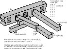
Figure 1: Pin Drive
A mechanical device driven by a sequence of simple digital commands will
have an internal state that changes with each command, and must be maintained
without error or slippage. Thermal noise injects constant vibration
into the system, requiring strong latching mechanisms. A simple latching
mechanism is a ratchet with a strong spring, as proposed by Drexler and
used by Merkle. A stepping drive can be built from two ratchets,
and early assembler designs that are controlled by simple external signals
may make extensive use of such drives. Such a mechanism is extremely
inefficient, since the energy used to compress the spring (at least 100
kT [Boltzmann's constant times ambient temperature] to overpower room-temperature
thermal noise) is lost each time the ratchet moves to the next tooth.
However, when a fabricator is connected to a digital logic system, the
fabricator no longer needs internal state-maintenance mechanisms, and the
device can be made far more efficient. (Digital logic, including
gates and registers, can be made thermodynamically efficient.)
An efficient drive with functional characteristics similar to the ratchet
drive is the pin drive. (See Figure 1.)
In this design, pins are inserted into equally spaced holes (or notches)
in the moving bar to assure its position at all times. The latching
pin moves in and out but not sideways, and is used to hold the bar still.
The driving pin moves in and out, and also is moved sideways by a bar actuator
over a distance equal to the spacing of the holes. The pins are similar
in structure and function to the rods in Drexler's rod logic design.
To move the bar one step, the bar actuator is moved to one end of its range,
pulling the driving pin into alignment with a hole. The driving pin
is inserted. The latching pin is withdrawn. Then the bar actuator
is moved to the other end of its range, bringing the next hole into alignment
with the latching pin, which is then inserted. Finally, the driving
pin is withdrawn and then moved back to its original position. Smaller
step sizes may be obtained by additional offset pins, or by a second vernier
drive, similar to the vernier ratchet drive described by Drexler (1992,
sec. 16.3.2), with slightly different hole spacing and bar actuator range
of motion from the main drive. Larger step sizes may be obtained
by moving the bar actuator a larger distance in each cycle.
Although the pin drive requires one more actuator than the ratchet drive--two
pins and a bar actuator, instead of two ratchet pawl pullers--it has the
advantage that it can move by measured steps in either direction, whereas
the two-ratchet drive can only move stepwise in one direction and must
retract in a single motion by lifting both ratchets. (If both pins
are lifted simultaneously, the bar can be moved without restriction by
a weak return actuator, allowing the same rapid return motion as the ratchet
drive. Note that without careful design, verifying the complete return
of the bar will require energy on the order of 100 kT.) Similar redesign
can be applied to any stepping drive mechanism. As long as the position
of the moving member is initially known, it can be moved stepwise, held
stiffly against thermal noise at every point, and locked in place in its
new position, all without irreversible state transitions.
While the pins are moving, the bar is stationary and the pins may be
moved reversibly. As the bar actuator is moved, the force encountered
may vary. Nevertheless, stiffly imposed motion will be efficient
in most cases. As long as the force profile of the motion does not
vary more rapidly per distance than the stiffness of the drive mechanism,
and does not vary substantially between forward and backward motion (e.g.
due to an irreversible state transition), it does not matter how much force
is required to move the bar at each point because the energy will be recovered
when the motion is reversed. This energy recovery requirement implies
that the drive mechanism must be able to recover energy from being driven
by the bar; such designs are not difficult, and include Drexler's electrostatic
motor/generator (1992, sec. 11.7). The same argument applies to other
types of actuators driven by other digital control mechanisms: as long
as the force profile is reversible and is less steep than the stiffness
of the drive mechanism, the energy that is put into the system is recoverable.
Note that rapid motion causes the force profile to deviate from reversibility
due to various energy dissipation mechanisms. (The author thanks
Eric Drexler for clarifying discussion of thermodynamic reversibility.)
3.2. Joining Product Blocks
There are several possible ways to join two mechanochemically fabricated
objects. Van der Waals force is an attractive force that develops
between any two nearby objects. For a few unterminated surfaces,
covalent chemical bond formation can in theory be used to make a seamless
joint. A wide variety of mechanical joints can be used. Section
3.2.1
describes a particularly useful strong mechanical joint, and Section 3.2.2
describes several press-fit joints for power, control, and fluid connections
between blocks.
At very small separations, two objects experience an attractive force
called van der Waals force: simply bring them close together, and they
stick. For two flat diamond surfaces, the force is approximately
1 nanonewton per square nanometer, or 10,000 atm of pressure (Freitas,
1999, sec. 9.3.2).
This is reasonably high, although it provides only a fraction of the strength
and stiffness of chemical bonds. The van der Waals force is the simplest
method of joining, it is reversible, and it should provide sufficient strength
to keep even kg-scale products from falling apart under their own weight.
This type of joint is convenient and can be used for weak joining of structures
that must later be separated.
A diamond surface that is not passivated with an outer layer of hydrogen
will be very reactive. Unterminated diamondoid surfaces forced together
should form covalent bonds. According to Drexler, two (110) surfaces
of tetrahedral diamond or two (100) surfaces of hexagonal diamond should
bond to each other on contact, forming a seamless joint (Drexler, 1992,
secs. 8.6, 9.7.3, and 14.2.1). Sinnott et al. (1997) report the results
of simulations that show bond formation, though not seamless joining.
For other diamond surfaces, or in the case of too-rapid joining, a somewhat
weaker joint may form with a lower bond density. Also, it is currently
unknown how much pressure would be required to initiate the process.
Crushing buckyballs to diamond requires 20 GPa, but Drexler states (personal
communication, January 24, 2003) that a covalent joint should "zipper"
itself if started at an edge or corner, that neon atoms should be able
to escape the closing gap and would not interfere with the joining, and
that argon is even better in this regard. If the joint were comparable
in structure to amorphous diamond currently made for MEMS, it would have
a tensile strength of only 8 GPa (Sullivan, 2002); this is significantly
less than diamond's tensile strength of 60 GPa (measured) to over 100 GPa
(calculated, depending on crystal orientation) (Telling et al., 2000).
An additional problem is that radiation damage or stray molecules may cause
local surface reconstruction or contamination that may hold surfaces apart
and prevent a joint from forming. This type of joint is usually not
reversible, though in theory a carefully designed edge might allow predictable
crack formation. Since seamless covalent joints have not yet been
demonstrated, the present nanofactory design does not use this method.
3.2.1. The Expanding Ridge Joint
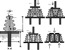
Figure 2: Expanding Ridge Joint
Each mating block face is covered with small "ridges" that are roughly
triangular in cross section. See Figure 2.
All exposed surfaces are non-reactive (e.g. hydrogen-passivated diamond).
The ridges on each face interlock with the ridges on the opposing face.
As the joint is pressed together, the ridges split and expand sideways.
The exposed surfaces of the ridges are not smooth, but are shaped to grip
the opposing ridge, with scallops deep enough to form overhangs when viewed
perpendicular to the block face. A scallop is chosen instead of a
sawtooth or ratchet profile in order to avoid crack formation at sharp
concave angles. Scallops also make assembly motions smoother, and
allow the un-powered assembly described below. The expansion of the
ridge opens a space in its center, which is then filled by a shim which
sits above the almost-closed gap between the two halves of the ridge.
Once the shim is in place, the volume of the joint cannot easily be compressed,
and the surfaces of the ridges cannot easily slide past each other; pulling
apart the joint would require compressing a solid mass of diamond by several
percent or breaking at least half of the ridges simultaneously. If
the ridges all run in the same direction, the joint may be able to slide
freely. Crossed ridges will produce a joint that is quite stiff against
shear.
The triangular shape of the ridges has several advantages. First,
the area of the base of the triangles (almost the entire area of the block
surface) is structurally solid. (By contrast, a square ridge would
waste at least half of the structural strength of the blocks being joined,
because the block area adjacent to the tops of the ridges would not contribute
to the joint.) Second, at small scales, van der Waals forces make
handling of components difficult because the components stick to any manipulator.
With triangular ridges and narrow ridge tops, the contact area of the surface
is much lower, reducing the van der Waals force. Third, a manipulator
can easily be aligned with the ridges. Small blocks can be picked
up by simple contact with a V-channeled manipulator that presents sufficient
surface area to form a van der Waals bond of the desired strength, and
the manipulator will automatically be pulled into alignment. A more
complex mating pattern could fasten on several ridges at once. If
the ridges are placed at varying angles or spacings, a well designed manipulator/ridge
interface can guarantee that a misaligned manipulator cannot form a firm
grip. Likewise, a well designed ridge/ridge interface can guarantee
that misaligned blocks will not join incorrectly.
There are at least three ways of mounting the ridge so that a small
attractive force between mating ridges will be sufficient to cause the
ridge to spread. The first possibility is to join the ridge to the
nanoblock with dovetail joints, permitting it to slide sideways with very
low friction. A simple dovetail joint costs somewhat more than half
of the possible joint strength; a stairstepped dovetail joint (which is
similar to a completed ridge joint) would recover much of the strength
at the cost of additional volume and complexity. The second possibility
is to use a mounting that is strong in tension but flexible in shear, such
as thin columns of diamond or buckytubes. The third possibility,
for use in linear stacks of many nanoblocks, is to build a solid structure
extending from the base of the ridge all the way through the block to the
ridge on the opposing face. Both ridges would move in tandem, and
be locked in place when the shims were dropped on each side. This
might require a mechanism for retaining all participating shims until all
joints are pressed together.
The simplest version of the expanding ridge joint requires no actuation
to form the joint other than moving the faces together. As the faces
are brought together, just before the final closure, each row of scallops
brushes past the inverse row on the opposing ridge. As the interlocking
ridges from each surface interpenetrate, the bulges of the scallops brush
past each other, close enough to be attracted by van der Waals force.
This pulls the halves of the ridge apart. The attraction between
passing scallops when the faces nearly touch must be stronger than the
intra-ridge attraction, to ensure ridge spreading during the last phase
of joint insertion, as the final rows of scallops pass each other.
This is ensured by the use of small spacers to control the van der Waals
force holding the intra-ridge gap closed. (The spreading will become
increasingly favorable as the faces approach, and the operation will happen
slowly enough to allow equilibration, so thermal noise will not cause the
joint to fail to close.) However, the intra-ridge attraction (between
halves of the same ridge) must be strong enough in the initial position
to prevent premature operation due to thermal noise. The half-ridges
must require a certain energy, say 100 kT, to pull them apart far enough
for the shim to be inserted; the displacement which absorbs this energy
cannot be greater than the depth of the scallop. Note that the required
energy is not dependent on any spatial parameter; it is related only to
temperature. However, the attractive force is approximately proportional
to surface area, so this condition can be satisfied by a sufficiently long
ridge joint. In other words, regardless of the actual inter-scallop
force, an intra-ridge gap can be chosen that will allow the ridge halves
to be separated; and regardless of the gap, a sufficiently long ridge will
be resistant to premature separation.
Due to the complicated geometry of the scallops, exact calculation of
the attractive force between mating ridge halves is beyond the scope of
this paper. An inaccurate calculation is given to permit crude estimation
of minimum ridge length. The formula for attraction between cylinders
(Drexler, 1992, Fig. 3.10f) will be applied, treating each scallop as a
0.5-nm radius cylinder separated by 0.3 nm. (This is inaccurate because
it ignores the attractive contribution from the material behind the cylinders,
and because the formula's derivation assumes that cylinder radius is much
greater than cylinder separation.) The inter-scallop potential energy
is calculated as 61 zJ per linear nanometer of scallop contact, which corresponds
to 2 nm^2 of surface between the two halves of the ridge. To reduce
the intra-ridge potential energy to 50 zJ per scallop-nm or 25 zJ per nm^2,
the spacing must be at least 0.6 nm (ignoring the attractive contribution
from the spacer) according to the formula in (Drexler, 1992, Fig. 3.10d)
which slightly overestimates the attractive force since the ridge is not
infinitely thick.
When the gap between the half-ridges is fully open, the shim (which
includes a hollow to accommodate the spacer) is pulled into the gap and
held there reliably by van der Waals force. The shim will insert
when the ridges have moved apart by a distance equal to the depth of the
scallop undercut, in this example 1 nm. With a 1-nm deep scallop
and a 0.6 nm initial gap (thus a 1.6-nm wide shim), the difference in potential
energy between 0.6 nm and 1.6 nm spacing is 21.5 zJ/nm^2. To prevent
premature insertion, the intra-ridge potential energy of attraction must
differ by 100 kT (260 zJ at 0 C) between closed and open positions.
This requires 12 nm^2 of intra-ridge gap. If the ridge is 8 nm high
(with 4 scallops), then it need only be 1.5 nm long.
The joint may be stiffened by compressing the joint volume. In
this case, extra force may be used to insert the shim into the gap.
(This also allows the gap to be somewhat narrower, reducing non-structural
volume.) A simple design for an electrostatic actuator adds only
one moving part. The shim is blanketed between insulated capacitor
plates, one of which is flexible. Charging the capacitor makes the
plates pull together, expelling the shim like a watermelon seed.
The electricity to power the actuator can be delivered through contact
with small embedded conductors at the proper time during the convergent
assembly process. The tip of the shim can be tapered to help spread
the ridge halves. Once the shim is expelled, the capacitor plates
will adhere to each other by van der Waals force, forming a reliable barrier
to hold the shim in the joint even if the capacitor is discharged.
Tension on the joint will tend to expand the entire joint volume sideways.
This can be constrained by surrounding each joint (not each ridge) with
a diamond collar sufficient to resist the sideways force generated by a
single ridge. The ridge joint is somewhat less stiff in tension or
compression than solid diamond would be, but should be almost as strong:
failure requires either significant compression of a large volume of diamond,
or the simultaneous failure of many covalent bonds. Effectively,
the entire joint volume except for the depth of the scallops and the width
of the shim contributes to the tensile strength, and the entire joint volume
except for the shim contributes to the compressive strength. Shear
strength and stiffness depend on the orientation and attachment of the
ridges, but can be made quite high perpendicular to the ridge line.
Torsional and bending strength and stiffness can also be made quite high.
The width of the shim is unrelated to the size of the ridge, being equal
to the depth of the scallop's undercut plus the intra-ridge van der Waals
gap. A reasonable lower bound for component size is a ridge composed
of four scallops 1 nm deep and offset by 1/2 nm horizontally and 2 nm vertically.
The height of the ridge is 8 nm, and the footprint of a half-ridge is 3.5
nm (accommodating 0.5 nm of motion to mate with the opposing half-ridge),
of which 2 nm contributes structural strength. The 1.6-nm wide shim
adds an additional 0.8 nm of non-structural overhead to each half-ridge;
the total joint tensile strength is approximately 47% of solid diamond.
(Shallower scallops will improve this number up to a point; scallops that
are too shallow can fail by slipping past each other.) For reliable
operation the ridge must be at least 1.5 nm long. The smallest joint
consists of one half-ridge on each side, only one of which (and its shim)
needs to move; the rest of the joint including the mating half-ridge can
be solid diamond. A single joint can potentially have a footprint
smaller than 3x6 nm. Larger ridges can have more scallops, with the
size of each scallop (and thus of the shim) staying constant. For
example, a half-ridge 20 nm high with 10 scallops has a footprint of 6.5
nm (plus 0.8 nm for its share of the shim) of which 5 nm is structural,
for 68% of diamond strength. Covering a 200-nm block with 8-nm-high
ridges on each side requires 8% of the block volume (ignoring block edges
and corners). However, in a high-strength application that requires
ridge joint coverage of the full surface, the block must be nearly solid
diamond anyway.
Because the strength of the joint decreases only slightly with smaller
size (the decrease is a function of the minimum shim, scallop, and van
der Waals gap size), small ridges are mechanically adequate for joining
blocks at any scale. Minimum ridge size is determined by the mechanochemical
fabrication process. The only limitations on block size are the precision
of the block-handling machinery and the possibility of unequal expansion
of the faces due to temperature differences. With 200 nm nanoblocks,
ridges built in a single block can be up to 100 nm in height, with tops
50 nm apart. (Note that the blocks will overlap by the height of
the ridge. The change in effective block width during assembly presents
issues for the assembly process that are straightforward but beyond the
scope of this paper.) An assembly tolerance of 0.05 micron is somewhat
beyond today's standards; current state of the art for automated pick and
place assembly for optical components appears to be around 0.5 micron (Blaze
Network Products, 2003). However, today's pick and place systems
use hardware made with a manufacturing tolerance comparable to its performance.
In contrast, the dimensional precision of the nanofactory's hardware will
be approximately one atomic diameter or less, regardless of scale.
At large scales, single ridges can be assembled from multiple nanoblocks,
allowing ridge spacing of multiple microns; this is sufficient even for
today's robotics.
Differences in fabrication processes, assembly processes, and internal
structure may cause different blocks to be at different temperatures.
The resulting thermal expansion can cause a misalignment of the ridges.
The volumetric thermal expansion coefficient of diamond is 3.5x10^-6/K
(Freitas, 1999, Appendix
A); the linear coefficient is one-third that, or 1.2x10^-6/K.
A temperature difference of 1 K thus causes a 200 nm block to expand by
a small fraction of an angstrom, while a 10.5-cm surface will expand by
126 nm. Because diamond is an excellent conductor of heat, passive
equilibration may be sufficient. As long as the displacement is not
greater than the ridge spacing, or the ridge pattern does not permit improper
joining, the blocks may be pressed together slowly, allowing the temperature
to equalize. Even a rarefied internal atmosphere will also facilitate
temperature equalization between nearby faces, though this process may
be slow depending on block mass, and the process will be somewhat slower
with argon than with neon. Note that the nanofactory is cooled by
phase transition (see Section 8.2), so the cooling
fluid will have the same temperature throughout the factory, minimizing
potential product temperature differences. Active compensation might
involve sensing the temperature at various points on the surfaces and applying
heat to the cooler surface via embedded resistive heaters; this will only
be necessary for the few large-scale joints that take place near the end
of the assembly process, and the heating process can be initiated in advance
to avoid delay. Embedded mechanical (bi-material) thermostats can
allow each region to reach a preset temperature without individual attention.
Because the joints require no external manipulation or assembly force,
they can be used to fasten non-bonded parts that are only loosely connected
to the main nanoblock. For example, a structural beam one micron
long and 50 nm wide can be constructed in five sections. Each section
will be terminated in ridge joints, and laid across a nanoblock in a position
that will place the section ends next to each other during block assembly;
van der Waals force will hold the section in place during block manipulation.
When the nanoblocks are assembled, the ridge joints of the beam will join
at the same time as the rest of the joints, with no additional effort.
This allows the inclusion of long, thin components in product designs.
Likewise, single nanoblocks can be made in separate pieces joined by van
der Waals force. This allows a block to be pulled apart during the
unfolding process, forming multiple walls with large spaces between them.
This can be useful to save mass where only thin walls are needed.
If a block is split into as many as 10 walls or 100 columns, the 20-nm
width is sufficient for multiple full-sized ridge joints on each part.
This capability is assumed for interior nanofactory structure.
Joints can be formed after the product is released from the factory,
as long as contaminants have been excluded from the joint space.
The factory can manufacture a larger containing balloon for product unfolding,
or the joints can be protected individually by a variety of covering mechanisms.
A product can be created in a very compact form, then unfold like a pop-up
book or like flat-packed cardboard boxes. Components can be built
in pieces, with lightweight pantographic trusswork to bring the ends together
as the product expands; once the ends touch, the strong joint will form.
A component can also be made in a "broken" state, with mating surfaces
held together on one edge with a small hinge at any desired angle, and
the open end protected by a bellows if necessary. When the component
is straightened, the mating surfaces will form the desired strong connection.
A weak and reversible joint can be formed by preventing the shims from
entering the gaps between the ridges. This allows blocks to be loosely
connected, then disconnected, and finally reconnected tightly in the same
or different configuration. This may be useful if the unfolding process
requires a structure to be produced in its final conformation, then flexed,
and finally fastened rigidly.
3.2.2. Functional joints
A product may contain embedded wires, pipes, rotating rods, nanocomputer
logic rods, and polyyne control cables. All of these may need to
make a connection between adjacent nanoblocks. These connections
are generally simple, and cost less than 50% of the performance that would
be possible with a seamless design.
Embedded wires can be run up to a flat face, and electrical contact
made by tunneling. Contact can be maintained in the case of joint
strain by the use of springy interfaces. According to measured values
for a sample of HOPG (highly ordered pyrolitic graphite), (GE Advanced
Ceramics, 2002) graphite is about 5000 times more conductive in-plane than
cross-plane (and the in-plane value is 1/50 as good as a typical metal).
The separation of graphite planes is 0.335 nm, about 1/600 of the 200-nm
nanoblock width. This implies that a graphite-graphite tunneling
surface of 8 nm^2 per nm^2 of graphite wire, spaced every 200 nm, would
only double the total resistance. To save nanoblock surface area,
the tunneling surface can consist of interlocking corrugations. Because
diamond is an excellent insulator, high voltages may be used to compensate
for the resistance of graphite. Some buckytubes may be better conductors.
Control cables and control rods will be built into each nanoblock when
it is manufactured, and extend only to its edges. Tension and/or
compression must be transferred between blocks. Nanocomputer logic
rods have ends ~1 nm^2 which can be butted together. The nanocomputer
design uses tensional force of 2 nN (Drexler, 1992, sec. 12.3.3.b) but
this can be traded for displacement or compressive force without sacrificing
reliability. Alternatively, the joint area can be increased by a
few nm^2 to allow a few nN of tensile force to be transmitted through van
der Waals attraction. Crossing between blocks may require adding
extra logic gates to transform and condition the signal; this logic can
all be reversible at some cost of time. Such interfaces will not
add significantly to the power requirements or design complexity of a nanocomputer.
Polyyne (carbon chains with alternating single and triple bonds) control
cables can be terminated with a small diamondoid plate flush with the nanoblock
surface. When the blocks are joined, the plates will stick by van
der Waals force. Each two atoms of polyyne spans a length of 0.2569
nm and has a compliance of 0.00185 m/N (Casing an Assembler, "Control cables").
A 1-nm diamond cube contains 176 carbon atoms. A van der Waals interface
has a stiffness of >30 N/m per nm^2 (Drexler, 1992, sec. 9.7.1), or a compliance
of <0.0334 m/N. Two hundred nm of polyyne contains 1557 carbon
atoms and has a compliance of 1.44 m/N, while 198 nm of polyyne interrupted
by two 1-nm diamond cubes interfaced by van der Waals force contains 1893
carbon atoms and has a compliance of 1.47 m/N; the interface increases
cable mass by 22% and compliance by 2% (ignoring the hydrogen termination
and internal compliance of the diamond cubes) and may introduce resonances
into extremely high-speed operations. The main drawback of the interface
is its strength; the tensile strength of a polyyne rod is >6 nN, but the
strength of the interface is ~1 nN. Increasing the interface area
allows a stronger and stiffer joint, and for joint areas above a few square
nanometers a ridge joint can be used at some cost of mass.
Power can be transmitted by means of thin rotating rods, embedded in
the nanoblocks like the control cables and logic rods. Mating convolutions
on rod ends will allow the transmission of torque between ends that are
simply pressed together. If the rod is driven near maximum torque,
the interface may need to be somewhat larger than the cross section of
the rod. The bursting speed of a disc decreases in proportion with
its radius, while the area increases as the square of the radius; thus
a 2x increase in interface area will cause a 1.4x reduction in speed.
In this simple example, power transmission is derated by 40%; however,
other mechanical linkages such as a thin belt connecting offset and overlapping
rods may permit full speed while delivering full torque. (The belt
can be placed around one rod during nanoblock manufacture and held open
by any of a variety of methods. The other rod can be tapered to slip
inside the belt during block assembly. Interlocking (gear-toothed)
rod surfaces will also work but may require significant overlap for reliable
torque transmission.) Rods and shafts larger than a few nm can be
joined by ridge joints. Ridge joints may also serve as a means of
chocking the shafts to ensure proper alignment, and then unlocking them
during convergent assembly: the shims can be inserted only when the joint
is fully closed, and the motion of their insertion can be used to remove
a mechanical chock. Small rods can be controlled by adjacent ridge
joints, and large shafts by facial joints with internal shims.
Bearing surfaces for rotating shafts small enough to be embedded in
nanoblocks can be built into each nanoblock during construction.
Variations in rod diameter will prevent the rods slipping out of the block
prior to convergent assembly. Large rods pose a special problem for
convergent assembly, since they cannot be strongly and permanently fastened
to a support or bearing structure. However, for products up to 10
cm size, a tight-fitting bearing surface between a rod and a housing can
provide the necessary adhesion by van der Waals force alone. Rotational
freedom can be constrained by small retractable chocks. Graphite
pads covering the matching surfaces of the blocks constituting the shaft
and the blocks constituting the housing can provide a bearing surface even
for slightly rough curved surfaces. However, the boundaries between
the pads will be aligned on the moving and bearing surface, and this can
create a significant force. (Twisting one of the surfaces relative
to the other would break the alignment, but this will not be possible for
cylindrical bearings.) Order-of-magnitude calculations can be made
by treating the boundary gaps as regions of wider spacing between the surfaces,
calculating the difference in van der Waals energy between aligned and
unaligned regions, and dividing that by the width of the gap to find a
force. Approximating the boundary as a trench 1 nm wide and 0.1 nm
deep and the pad spacing as 0.2 nm, and applying the formula from (Drexler,
1992, Fig. 3.10d), indicates an energy difference of 81 zJ per nm^2 in
favor of the aligned state, or an average force of 81 pN per linear nm
of trench. One mm^2 of flat sliding surface will contain 5x10^9 nm
of trench crossing the direction of motion, creating a force of ~0.4 N.
However, the stiffness of 1 mm^2 of graphite bearing surface is ~3x10^13
N/m, so for many macroscopic applications, bearings may be made small enough
that the "roughness" is not a significant problem. A cylindrical
bearing surface cuts across two nanoblock planes and only a fraction of
the area contributes to stiffness; these factors increase the number of
trenches (and thus the "roughness" force) for a given bearing stiffness
by approximately a factor of 4.
Pipes are simply voids in the diamond nanoblocks that are butted together
when the blocks are assembled. A flat, uncompressed interface between
nitrogen-terminated diamond (111) surfaces is adequate to exclude helium
(Drexler, 1992, sec. 11.4.2a). If this type of interface proves inadequate
in practice (perhaps due to joint flexure, or unavailability of nitrogen
termination chemistry), a conical extension of the pipe wall wrapped in
one or more layers of graphite to provide a compressive seal and extending
into a conical depression in the other block should suffice. Pipes
too large to be contained inside a nanoblock can be sealed by diamond or
graphite curtain walls, placed along each seam, to separate the interior
of the pipe from the mechanical joint area. If the nanofactory is
filled with inert gas, pipes will also be filled with the gas when they
are manufactured. If this is a problem, one possible solution is
to place a collapsed graphite tube inside the pipe, terminating the tube
ends at the nanoblock faces with a diamond mating collar thin enough to
be flexible. When the blocks are assembled, the collars join.
When first used, the graphite tube will expand and conform to the walls
of the pipe while displaced gas can be vented through small channels.
4. Nanofactory Architecture
A nanofactory, as conceived here, is a single device containing many mechanochemical
fabricators and larger-scale manipulator systems. The mechanochemical
fabricators produce nanoblocks and the manipulator systems join them into
a product. The mechanochemical working space of a nanofactory must
contain no stray reactive molecules. The factory must contain computers
to control the machinery; space and mechanisms for convergent assembly;
structures for distributing power, chemicals, and cooling fluid; mechanochemical
fabricators with space for them to work; and additional space for joining
blocks into larger blocks and transporting them through the factory.
The nanofactory is built hierarchically, using only a few scalable designs.
At the lowest level, a few thousand fabricators are arranged in a planar
grid. Their products are picked up and assembled into increasingly
large blocks by a series of increasingly large robotic manipulators.
This plus a control computer constitutes a basic, reliable production
module. The production modules are stacked three-dimensionally
into gathering stages, which assemble blocks and pass them to higher-level
gathering stages. Finally, the entire factory is enclosed in a suitable
casing, with a mechanism to output product without contaminating the workspace.
In Merkle's convergent assembly architecture (1999) it is suggested
that each convergent assembly stage has four inputs, each supplying two
blocks to make one output block. However, this means that each input
to the preceding stage must supply four blocks to make those two, and so
on. This is feasible if blocks can be manufactured extremely quickly,
or (as in Merkle's design) fed through a relatively small number of ports
efficiently. The current design, using large nanoblocks requiring
minutes or hours to fabricate, uses only one block from each fabricator
per product cycle. This implies that each stage will receive all
its blocks in parallel. In general, then, each stage must have either
eight (non-redundant) or nine or ten (redundant) inputs. (The first
gathering stage has only four inputs, to compensate for the eighteen inputs
of the final stage in the production module; see below.)
4.1. Mechanochemical functionality
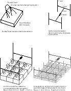
Figure 3: Workstation Grids
Once a self-contained, digitally controlled mechanochemical fabrication
system has been developed, the fabricator design can be copied directly
from it. Early systems will presumably use a simple, stiff robot,
such as a double tripod (Merkle, 1997c) or Stewart platform. As noted
in Section 8.2, any inefficient ratchet or other state-keeping
systems in the fabricator can be replaced with thermodynamically efficient
stepping drives. Even with this improvement, the primitive method
of mechanochemistry will cost some efficiency relative to the "mill" type
designs analyzed by Drexler (1992, sec. 13.3) and used in his nanofactory
design (1992, sec. 14.4). Because placing each atom or molecule requires
a large and complicated motion of the tripod system, the nanofactory will
suffer some penalty in both speed and energy use; these penalties are substantial
but not crippling. Mills are not included in this preliminary design
because they may require significant additional mechanical and mechanochemical
design.
Fabricators will be fastened together edgewise to form the planar array,
which divides the coolant volume from the working volume. Cooling
fluid with dissolved feedstock circulates past one side; the products (nanoblocks)
are fabricated and released on the opposite side, which is open to the
nanofactory's clean working volume. A square of nine fabricators
(one redundant) forms a stage. Product blocks are picked up by a
three degree of freedom gantry crane manipulator and assembled into a 0.4-micron
block. Likewise, a square of nine of these stages forms the next
stage. This continues through several levels; in the current design,
four levels is chosen for suitable redundancy and convenient control.
4.2. The reliable basic production module
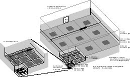
Figure 4: Production Module
A production module fabricates two 3.2 micron product blocks out of up
to 8,192 nanoblocks, using a fabricator to produce each nanoblock.
The module is extremely reliable in the face of radiation damage, and is
controlled by an integrated nanocomputer. The overall shape of the
module is a rectangular solid ~16x16x12 microns. The fabricators
are placed on two opposite sides, delivering their product nanoblocks to
the interior. The nanocomputer occupies a third side, surrounding
the product exit port. The remaining three sides may be closed by
thin walls, but need not be closed at all where two production modules
are placed side by side in the nanofactory. The interior is sparsely
filled with gantry crane manipulators to assemble the nanoblocks into larger
blocks. The gantry crane mechanisms, even at the smallest scale,
can be implemented as bulk diamond machines--the smallest blocks are 200
nm on a side, and bulk diamond parts can be designed far smaller than that,
so not much material or volume will be wasted due to inefficient design
constraints. With the ridge joints, the blocks can be assembled simply
by bringing them into contact (Section 3.2.1).
Rotation of blocks will not be necessary because each block (or partial
block) can be manufactured in the same orientation it will take in the
final product (before unfolding). The design of the ridge joints
provides a rough surface that can be gripped with as much force as necessary
to accelerate the cubes and (depending on scale) overcome gravity.
The physical layout is similar in some respects to Merkle's architecture
for convergent assembly (Merkle, 1999). Substage outputs are be grouped
on one wall of an assembly chamber, forming the inputs to the stage; substages
are placed side by side, and stages are stacked on top of substages.
See Figure 4. As in Merkle's design,
the output from a stage is twice the width of each input; unlike Merkle's
design, each input port delivers only one block per product cycle instead
of two. The design is not quite scalable, since the width of the
assembly stage is three times the width of the sub-stage, while the width
of the block that is produced is only two times the input block size.
The ninth substage is redundant, used in case of failure of another substage.
Four levels of redundancy are probably sufficiently redundant for a nanofactory
of the size contemplated here. Otherwise, more redundancy can be
added in a fifth stage, or by extending a gathering stage; see Section
8.5
for calculations.
The module's top and bottom surface are completely covered with 9^4
= 81^2 = 6561 mechanochemical fabricators each. To provide space
for moving sub-blocks around a growing assembly, each stage is 3.1 times
as high as the sub-block it receives. Two of these assemblages are
sandwiched together, sharing a single 3.2-micron assembly stage, to make
one production module that produces two 3.2-micron blocks per product cycle.
The design can be compacted somewhat if multiple convergent assembly stages
can be combined; such optimization is beyond the scope of this paper.
The CPUs, memory, DMA controllers, and motors are placed on the face that
contains the output port, forming a single layer and extending the width
by 0.2 micron. Controlling a column of 81 fabricators requires perhaps
a few billion bits per second and <100 pW (Section 8.2),
which fits through an interface requiring only a few nm^2. Only 4096
fabricators per side are used at any time; the rest are redundant, to be
used in the event of radiation damage. See Section 8.5
for further discussion of this design. Powering the entire set of
8192 fabricators plus the computer requires 8 nW, far smaller than the
500 nW capacity of a single electrostatic motor.
4.3. Gathering stages
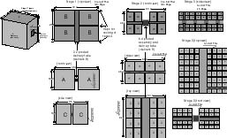
Figure 5: Convergent Assembly Fractal Stages
The production module is scaled to tabletop or larger size with a simple,
repeatable architecture. Each gathering stage fits neatly into a
rectangular solid, with the substages arranged in two rows on either side
of a central assembly and transport tube. The substages, themselves
rectangular solids (including the production module), fit together with
no wasted space in each row. Space is wasted between the rows, adjacent
to the central tube. Gaps are left for feedstock/cooling channels
adjacent to certain faces of the production modules. Wherever no
gap exists between substages, no walls are necessary. As the modules
are stacked, the cooling channels line up; the overall arrangement is a
quasi-fractal working volume interpenetrated by a non-fractal cooling channel
volume. Power and signals are routed through the walls of the transport
tubes, since the end of every transport tube touches the side of the next-larger
tube. Power can be distributed through rotating rods or conductive
graphite or buckytube inclusions (wires) in the structural diamondoid blocks.
Control signals can be sent mechanically through polyyne rods, or electrically
through wires. The current design does not require fractal distribution
of liquids, since feedstock is dissolved in the cooling fluid. Inspection
of Figure 5 shows that some coolant channels
will be blocked by assembly tubes in stages with numbers divisible by 3;
this requires a gap between the sub-stages and the tube that is a fraction
of the cooling gap width, which is not included in the present calculations.
It may be desirable to prevent fluid from flowing into large voids adjacent
to the delivery tubes, to prevent excessively slow flows that could allow
suspended particles to settle out. More detailed design is beyond
the scope of this paper.
The factory does not require a hierarchical network of computers, since
the computation is done either at the top level or at the level of individual
production modules (see Section 6). Once the blocks
are fabricated, a fraction of the production module computers can be used
to run the convergent assembly robotics. If hierarchical computers
are needed, the computers can be built into the tube walls. Amplification
will be needed to distribute the top-level signal to each of the production
modules. This can be implemented in each stage, and can be combined
with a mechanism to send a unique, hard-coded position indicator to each
production module. By knowing which branch the signal takes at each
stage, the module's computer can easily determine the position of its output
in the final product.
A tabletop factory might produce a 10.5-cm product; this is 2^15 times
larger in linear dimension than the 3.2 micron output of a production module,
so product assembly requires 14 further assembly stages where each stage
assembles 64 sub-blocks to produce eight product blocks. See Figure
5, and Section 8.3 for dimensions. A final
stage, external to the factory, is described in the next section; it assembles
eight 5.25-cm sub-blocks (per product cycle) to produce the final product.
Note that the first stage in the Figure is not an assembly stage, but serves
only to gather 8 sub-blocks for delivery to the next stage, since each
production module makes only two blocks per product cycle. Each assembly
stage gathers 64 sub-blocks from substages, assembles them within the assembly/delivery
tube, and delivers the 8 assembled blocks to the superstage. With
the current size parameters, in some of the smaller stages, a minimum-volume
arrangement leaves the tubes perhaps too short for simultaneous assembly
of 8 blocks. Four blocks may have to be assembled and passed on to
the next stage, and then the other four assembled; this adds only fractionally
to the total product cycle time. The Stage 1 delivery tube is fractionally
larger than the 3.2-micron product it carries. The other assembly/delivery
tubes are large enough to allow moving sub-blocks to fit past the product
block under construction.
4.4. Casing and final assembly stage
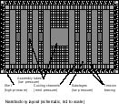
Figure 6: Nanofactory Layout
The nanofactory must maintain its structure against atmospheric pressure,
internal pressure differences, its own weight, and the weight of its products.
Loads can be more efficiently carried in tension than in compression, since
tension members do not have to resist buckling. Low-pressure internal
volumes (the fabrication and assembly space) are kept from collapse by
cables/braces stretched across the higher pressure volumes (the cooling
channels); see Figure 6. The whole thing
is suspended from a rigid exterior shell. For flexibility, the chosen
design includes a capability to do final assembly and unfolding in a protected
volume external to the factory itself, which can be of arbitrary size.
The overall nanofactory shape is a rectangular solid. The exterior
shell consists of six flat panels enclosing the necessary volume.
Each panel provides support to anchor the interior and prevent the working
volume from collapsing under atmospheric pressure. (Cooling fluid
pressure will be contained by the tension members crossing the cooling
gaps, and will not put additional force on the external casing.)
This is equivalent to a 1-atm pressure difference between the inside and
outside of each exterior panel, imposing a bending force. In addition,
the panels support each other, experiencing a crushing force at each edge.
The panels are hollow and pressurized. Internal tension members,
set at a slight angle, keep them rigid and flat. Since the working
volume contains the lowest pressure in the nanofactory, no pressure bracing
needs to be installed inside that volume; the cables only intrude on the
cooling channels. With many small cables supporting them, interior
walls can be very thin. See Sections 8.2 and
8.3
for a discussion of structural mass and coolant and panel pressure.
Sufficiently numerous and thin cables (no thicker than the walls) cannot
tear the walls; since the cables can be as thin as a buckytube, details
of attachment need not be considered.
In the final gathering stage, multiple blocks (up to 8 per product cycle)
are pressed together to form the final product. The product must
be delivered without allowing contaminants into the factory. One
way to do this is to produce a rectangular solid extruded through a sliding
seal, as in the "replicating brick" approach of Merkle (Drexler, 1992).
This constrains product configuration, requires that all faces be smooth,
and does not provide a protected environment for post-assembly unfolding.
An alternative design, permitting much greater flexibility in product shape,
is to enclose the final stage in a balloon, the neck of which forms a sliding
seal with the factory. A new balloon is installed for each product,
pushing the old one (with previous product) out and preventing contamination.
The mechanism of the final assembly stage must be extended for some distance
outside the factory during final product assembly, but still requires only
three degrees of freedom. Once the product is assembled and optionally
unfolded, the assembly mechanism is retracted and a new balloon is installed.
Most of the nanofactory mechanism is maintained at low or zero pressure
to reduce drag on moving parts. To allow balloon inflation, the final
convergent assembly tube is used as an airlock, pressurizing it with pure
neon or argon after all 64 sub-blocks have been delivered.
If low pressure in the factory is tolerable, the airlock need not be scavenged
completely before the end of the next product cycle, and mechanical pumping
will be sufficient. If even a few atoms of noble gas cannot be tolerated
in the factory or included in interior voids of the product, the airlock
can be scavenged by use of a cryogenic surface; since neon and argon do
not adsorb at room temperature, "bake out" is unnecessary and the airlock
can be completely emptied of gas in a relatively short time. The
design of the assembly mechanism, airlock mechanism, and balloon installation
is straightforward.
4.5. Issues in bootstrapping
Initial stages of bootstrapping will benefit from an ability to directly
observe and connect with individual fabricators. (Direct contact
is not a given for all designs; for example, Merkle's assembler floats
in a solvent, which limits both the complexity and the bandwidth of communication
with it.) Interfacing with a single 200-nm fabricator will require
some delicate lab techniques, which may not be worth the effort, but are
discussed here to illustrate the feasibility of control at that scale.
This section describes how a single 200-nm fabricator can be supplied with
power and feedstock in a dry environment suitable for immobilizing and
imaging the fabricator.
Several imaging technologies may be useful. Electron microscopes
have a very fine resolution and form images rapidly, but use multi-keV
electrons. Single-wall nanotubes can be imaged in an electron microscope
without apparent damage, but high-energy electrons may penetrate a single
graphite layer and either do chemical damage to sensitive bonds or charge
insulating surfaces, which could cause undesirable electrostatic forces
that would probably interfere with operation. Vapor deposition of
metal on the outer surface of the fabricator before imaging may alleviate
this problem. Scanning probe microscopy may be useful for imaging
the probes as they are aligned with the fabricator. Non-contact AFM
(atomic force microscopy) can avoid displacing the probes due to contact
forces. Optical interferometric methods may be useful for feedback
on at least one dimension of alignment. Finally, two-part fluorescent
systems (e.g. absorber and fluorescer, or absorber/fluorescer and quencher),
with one part attached to the fabricator and the other attached to the
probe, may be useful for final alignment (Drexler, 1992, sec. 16.3.6c).
The number of probes to be attached is small--only four for the first several
bootstrapping steps.
The moving-plate electrostatic actuator described in (Drexler, 1992,
sec. 11.6.4) requires a plate area of only 150 nm^2 and provides 1000 zJ
per actuation. A 100 MHz cycle time requires 100 pW. The actuator
is powered by 5 volts, requiring a current of 20 pA. This current
is far lower than the 0.1 mA that has been measured in a single buckytube
(Ipe Nanotube Primer, 2001), so buckytubes can be used to deliver power
for initial bootstrapping stages. A manipulation system like the
Zyvex three-probe SEM manipulator (MinFeng et al, 1998) can place buckytubes
with 6-nm precision on separate pads on the fabricator. A ground
connection can be made through the surface the fabricator rests on.
This can supply power for several actuators, which can control any number
of internal systems if one of the actuators is used to drive a simple mechanical
selector.
If the fabricator is in a dry environment, feedstock must be delivered
via a closed system. Hollow glass needles can be drawn as fine as
30 nm (Intracel LTD, 2001) which is small enough to interface directly
with a single fabricator. Two needles are needed to maintain a flow
of fresh solvent past the molecular intake port; this accommodates designs
that reject waste molecules as well as designs that use varying amounts
of multiple chemicals during the fabrication process. A housing over
the molecular interface with two 40-nm holes partially closed by 10-nm
graphite sheets should allow a leak-proof, though not strong, interface
to the needle tips. The tips can be positioned using the same kind
of manipulator used to position the buckytubes, and held in place during
the fabrication operation.
A single fabricator has space inside its casing to make two duplicates
with separate shells. Instead, it could fasten the two together,
side by side, and combine the shells. This would give roughly four
times the internal working volume for the same area of shell, and the two
fabricator stages could each produce two 200-nm blocks. A single
additional ratchet would select whether the actuation was to be delivered
to one or the other fabricator, or both together. (Either the electricity
or the resulting mechanical motion could be switched.) Most of the
time, both fabricators could be working in synchrony, so the same control
signals could be routed to both of them; duplication time would not be
greatly increased.
Since the two fabricators are placed side by side, their products would
also be adjacent. When fabrication was finished, each double tripod
would have sufficient range of motion to grab its finished product and
move it into contact with the other. A single 1 nm^2 contact area
would apply 1 nN of force. The weight of even a 10-micron cube, containing
125,000 nanoblocks, is 0.035 nN, allowing over 10 gravities of acceleration.
With small step sizes, torsion from off-center moving force can be relaxed
after each step; since only a single motion of a few nm is needed, this
will not significantly affect duplication time.
As the device grows, more different kinds of blocks will be required,
but more electrical control channels can be added. Blocks containing
convergent assembly manipulators will be mostly empty space, so will not
require much fabrication time to complete if they must be built one at
a time. An internal CPU will not be required until the stage where
it is a small fraction of the overall device mass. Once the device
is sufficiently large that at least six control channels can be attached,
the manufacture of the CPU and RAM can proceed in parallel with the manufacture
of the fabricator blocks without affecting duplication time.
There are many suitable physical layouts for the medium-scale devices.
For example, mechanochemical modules could form plates to line the top
and bottom of a wide workspace, with the plates separated by 800 nm.
Each module would make two nanoblocks, extending them vertically into the
workspace until they touched the nanoblocks from the opposite side.
The resulting product would be four nanoblocks thick; each face of the
nanoblocks would be either strongly fastened to its neighbor or weakly
held by van der Waals forces. When the product was completed, the
tripods working in concert would pass it out one side of the factory which
would open onto a balloon large enough for the product to unfold into a
flat factory of twice the area. A slightly more advanced design stacks
several of these flat factories and includes a 1 DOF (degree of freedom)
manipulator extending into the balloon to push together (and thus join)
the product slabs after they have been extruded; this allows more complex
unfolding. The maximum workable size of this design is limited by
radiation damage. A factory of 16,000 fabricators (a suitable size
for one nanocomputer to control, with the program downloaded in stages
to save memory) may have a 1% chance of suffering a disabling hit to a
single fabricator in a single day (see Section 8.5).
4.6. Improving the design
The mechanical format of the nanofactory can be improved by reducing the
empty volume. Since block assembly does not require much time, then
if manipulators can handle two or more block sizes the factory size can
be reduced by converting some of the assembly/delivery tubes into delivery-only
tubes of ~1/3 the width, and implementing multiple assembly stages in the
other tubes. Stages may also be re-used in the production modules,
making them flatter.
The current design is extremely wasteful of power. It is also
limited in the speed at which it can work. The inclusion of "mills"
for early-stage chemical processing (Drexler, 1992, sec. 13.3) can save
orders of magnitude of power and significant time. A mill does not
require any computation to perform an operation. Additionally, a
mill can more easily recover energy from exothermic reactions, and even
from the final stages of endothermic reactions. With mills preparing
small diamond cubes or hexagonal carbon chains that can be covalently bonded
to each other (Drexler, 1992, sec. 8.6.5b), a hybrid mill/manipulator system
could produce bulk diamond far more quickly and efficiently. Because
mills require both mechanical and chemical design, they have not been included
in the current nanofactory design.
The inclusion of atoms other than carbon and hydrogen allows flexibility
of design. In particular, Kaehler brackets (1990) would allow more
precise designs of surfaces and orientations. To some extent, mechanochemistry
can be developed by simulation in advance of fabricator availability.
Even without using additional chemistry, stepwise actuation can be made
more efficient and faster. Current design requires a separate operation
for every step, and each operation requires computation and time.
A non-stepping mechanism might be an improvement. For example, a
set of stops could be included in the path of a sliding bar. A chosen
stop would be extended, all other stops disengaged, and a linear actuator
used to move the bar rapidly until the stop is contacted. The force
profile of the actuator is problematic. For efficiency, its force
must be weak over most of the displacement, but for resistance to thermal
noise, it must apply a strong force at the end of the cycle. (A combination
of a weak actuator and a slow but strong latching pin may also be efficient.)
An alternative is to use several drive mechanisms with varying step sizes,
some of them large, or to design the pin drive so that in a single cycle
it can move either one or several steps.
Many other mechanical and chemical improvements will be obvious.
The development of improved nanofactory models may be expected to proceed
quickly, and manufacturing performance will also increase quickly.
Performance of products will increase somewhat as a result of continued
research and development. By several measures, products produced
by the current nanofactory design are already within an order of magnitude
of theoretical limits. It should be noted that no part of the current
design requires such levels of performance.
5. Product design
This section discusses the design of nanofactory products, including design
constraints imposed by the use of nanoblocks, in sufficient detail to encompass
nanofactory design. Section 5.1 discusses various
levels of design. The design process is simple enough that a CAD
(computer aided design) program to support each of these levels will be
fairly straightforward, so is not addressed here. However, since
the decoding of a product specification may use significant energy, the
design strategy is developed in sufficient detail to permit rough calculations
of the energy cost of internal nanofactory control (Section 8.2).
Capabilities developed in order to design a nanofactory may also be useful
in designing other products. The discussion of general product design
may be useful in forecasting the economic value of a nanofactory of this
type, although such forecasts are beyond the scope of this paper.
Section 5.2 contains a brief discussion of simulation
and testing.
5.1. Levels of design
Even a microscopic product may contain trillions of atoms. It is
clear that direct human effort cannot specify each atom separately.
The solution adopted here is re-use of components for multi-scaled designs:
a few components at one scale can be combined in many ways to make many
larger-scale systems. The nanofactory can be designed using six levels.
First, mechanochemistry creates nanoparts. The parts are combined
into nanomachines, which are fitted into nanoblocks.
Combinations of nanoblocks specify patterns which are used to fill
regions.
Finally,
folds are built into the product to allow it to unfold
and rearrange into more complex shapes and larger volumes. Each of
these levels can be designed almost independently of the others, and each
can be efficiently encoded into a product specification file and decoded
to control the nanofactory. Additional methods of design, which may
be useful but are not required for the nanofactory, are covered briefly
in Section 5.1.6.
5.1.1. Nanoparts
A certain level of mechanochemistry research will have been accomplished
in the course of creating the fabricator. This will probably include
the ability to build diamond lattice in a variety of shapes. Since
diamond lattice is repetitive, the motions required to fabricate it are
almost certainly also repetitive. Simple bulk diamond parts may be
specified by volume, requiring very little information to encode an arbitrary
number of atoms. (J. Soreff points out that the position of atoms
may be distorted by proximity to an edge, though this will probably require
only predictable displacements of mechanochemical motions.) Likewise,
buckytubes may be specified by chirality and length. Parts with complicated
surfaces, or that involve an interface between diamond lattice and some
other molecular structure, may require a listing of individual atom positions
or even of individual fabrication motions. It is unknown what percentage
of the fabricator will be bulk diamond. However, non-fabricator components
of the nanofactory can generally be built out of some combination of bulk
diamond and reused fabricator parts.
One of the most complex components of the nanofactory will be the nanocomputers.
A nanocomputer of Drexler's design (1992, chap. 12) consists of only a
few types of parts, including logic rods with varying combinations of knobs,
a few kinds of springs, cams, a motor/flywheel, and a housing.
Although the computer may contain thousands of different rod configurations,
all rod designs can be synthesized from knobbed and knobless segments;
each additional rod thus requires only a few bits to specify knob positions.
Assembly of the parts into the nanocomputer will also be repetitive, as
much of the circuitry consists of regular arrangements of rods in programmable
logic arrays. Translating from a digital logic specification to a
mechanical hardware arrangement is straightforward.
Mechanical devices large enough to be specified with bulk diamond construction
are also large enough that their strength and stiffness can be treated
with classical approximations (Drexler, 1992, chap. 9). Although
other effects such as electron tunneling between conductors may be significant,
a purely mechanical design can usually ignore them. The main difference
between nanoscale mechanical design and macroscale design will be surface
effects including van der Waals force.
Nanopart designs may be parameterized. For example, instead of
a different part specification for each length of buckytube, a single specification
can be given with a start, a finish, and a middle component that can be
repeated as desired. The nanocomputer logic rods are another parameterized
part. It should be possible to specify complex volumes of diamond
in terms of geometric description. As discussed in Section 6,
the choice of whether to parameterize a part or to specify its variants
separately will depend on a tradeoff between processing power and memory
space.
5.1.2. Nanomachines
Once fabricated, nanoparts are assembled by the fabrication system (e.g.
double tripod) into sub-components such as programmable logic arrays and
actuators, and eventually into nanomachines such as computers and double
tripods. Industrial robots perform similar tasks today. Van
der Waals force allows weak joining, and the ridge joint (Section 3.2.1)
allows strong joining for parts over a few nanometers in size. In
general, the assembly process will not require techniques analogous to
welding, gluing, or the use of small fasteners such as threaded bolts (Hall,
1999).
The level of nanomachines is not strictly necessary; parts could be
assembled directly into nanoblocks. However, the use of this level
of specification causes no loss of capability and is convenient since human
designers think in terms of machines. A nanomachine specification,
then, includes some sequence of nanoparts and sub-components together with
a sequence of assembly operations that assemble the sub-components.
Sub-components may be considered as nanomachines in their own right; this
saves space in the product description file, as one sequence of parts and
operations can be included in several machines by reference.
5.1.3. Nanoblocks
During a product cycle, fabricators in the nanofactory make a single nanoblock
each. Unlike nanoparts and nanomachines, the size and shape of nanoblocks
is more or less fixed. A nanoblock is small enough to be made rapidly,
but large enough to contain useful functionality. What varies is
the contents of the block and the surface connections to adjacent blocks.
Within some limits (to allow handling by the convergent assembly mechanism),
partial nanoblocks can also be built; this is useful in making smoother
surfaces.
In the current nanofactory design, a nanoblock is a 200-nm cube.
If a typical diamondoid part occupies a 10 nanometer cube (which has space
for ~176,000 diamond-lattice atoms) then 8,000 parts can fit inside each
nanoblock. For comparison, a typical 4-cylinder automobile engine
has ~450 parts (Whitney et al., 1998). As in the nanocomputer design
(Section 6.1), where the CPU occupies one cube and
memory is placed in adjacent cubes, designs can often be broken along convenient
planes and placed in adjacent cubes, communicating through pipes, small
control rods, electrical wires, or larger mechanical interfaces.
The simplest nanoblock is inert--solid structural diamond, with full
structural ridge joint coverage at one or more faces. Another class
of nanoblock is filled with digital mechanical logic; several nanoblock
designs are needed to implement a nanocomputer. A third class of
nanoblock could be filled with actuators; a nanoblock full of electrostatic
motors could convert a microwatt, and the same block would function as
an electrical generator without modification. Any nanoblock design
could contain some volume for miscellaneous functionality such as a few
gates of digital logic, a fan-out of a control cable with signal amplification,
or simply passing a signal through; reserved volumes that are continuous
between various block faces would be especially useful. A fourth
class of block would contain just enough diamond for rigidity of faces
and support of interior structure; this would be used mainly to contain
predefined nanomachines in novel arrangements, or to support convergent
assembly operations. Miscellaneous functionality could be specified
by direct design, or by semi-automated design using macros and automatic
placement and routing. (In constrained volumes automatic placement
would be more difficult.) Predefined blocks and block classes could
be extensively tested. Spatial separation of functional units, either
within or between nanoblocks, will reduce unexpected interactions.
Thus, most if not all nanoblocks in a product will be pre-designed (or
contain predesigned components arranged according to design rules), easy
to specify, pre-tested, and highly reliable.
5.1.4. Patterns and Regions
A 10.5-cm cube contains 144 quadrillion nanoblocks; the designer cannot
specify each one by hand. Much of the design will be repetitive,
and patterns and regions allow the specification of repetitive patterns
of nanoblocks. A pattern is a shape that is composed of multiple
nanoblocks. A region is a semi-arbitrary volume that can be filled
by patterns. Such specification allows large volumes to be filled
with very little specification data. (In the simplest case, one nanoblock
specification and one number can define a cube of any size.)
The simplest pattern consists of a single nanoblock type, with faces
compatible with stacking. More complicated patterns may specify repeated
or tiled arrays of different nanoblocks; these may be used to implement
(for example) a material with embedded strain sensors. Patterns may
be one-, two-, or three-dimensional, and may be designed to stack either
with themselves or with other patterns. Pattern specification can
be recursive: patterns can include smaller patterns or regions. In
the design of the nanofactory, each convergent assembly stage can be represented
as a single pattern, consisting of eight copies of the sub-stage pattern,
plus the walls, braces, and assembly tube required to connect them.
Patterns of nanoblocks can be tiled to form virtual materials occupying
regions. For example, a structural material could have a nanocomputer
per cubic millimeter, connected into a 3D grid, and strain sensors embedded
in various nanoblocks. A design for a single display pixel could
be tiled to form a raster display of any desired size. A useful CAD
program will allow such materials to be designed, and then used to fill
specified volumes; by this method, large, simple products can be specified
with very little design effort and small file sizes. (In any case,
the size of the specification depends on the complexity, and not the size,
of the region.) A more sophisticated program would allow the algorithmic
specification of complicated volumes, such as fractal trusses. The
nanoblock width of 200 nm is 100 times less than a typical human cell (Freitas,
1999, table 8.17);
for most human purposes, a material specified in terms of whole nanoblocks
would appear smooth, but partial blocks could be made as long as the convergent
assembly mechanism was still able to grip them as needed. Some machinery
such as large cylindrical bearings will be improved by partial nanoblocks;
lining the bearing surface of each block with graphite sheets will smooth
out any rough edges left by bulk diamond fabrication. (See Section
3.2.2).
For convenience in packing products more compactly, a simple extension
of the concept allows two different patterns to specify different fractions
of a nanoblock's contents; this allows patterns to interpenetrate or to
stack tightly, and can be used to specify small parts attached to nanoblocks
during fabrication but removed during unfolding.
Although the volume of nanotech-built machinery is far smaller than
the conventional machinery required to perform a comparable function, some
provision for redundancy will be required above the nanoblock level.
For example, generating 1 W of mechanical power requires perhaps two thousand
cubic microns of electrostatic motors, which may receive a damaging radiation
hit every few days (see Section 8.5). The process
of combining functional modules into larger modules that are tolerant of
radiation will be a common design pattern. The larger modules can
then be combined into a second-order virtual material, if desired.
During convergent assembly, the product is assembled from sub-blocks
into larger blocks. Thus a 10.5-cm product is assembled from 5.25-cm
blocks, which are assembled from 2.635-cm blocks, and so on. However,
the boundaries of patterns, and of regions, need not correspond to the
assembly boundaries. With ridge joints, nanoblocks can be assembled
simply by moving them into contact. This implies that any pattern
should be able to be split along any assembly boundary, or conversely,
that assembly boundaries can fall anywhere in any pattern. In practice,
two difficulties arise which may require some accommodation of the assembly
method, depending on the product.
Spaces within a pattern or around a region may be left empty of nanoblocks.
A void may cause an assembly failure because of a thin or unattached piece
adjacent to an assembly boundary. Voids do not pose severe problems
for the nanofactory design. The nanofactory, as fabricated, will
not include large voids, since it will be unfolded after fabrication (see
section 5.1.5). In product designs requiring
voids, the voids may be filled with a scaffold of mostly-empty nanoblocks
that can fold out of the way after construction.
Another difficulty is that assembly of large blocks may not allow sufficient
precision to use ridge joints only a few nm in size; it is not yet known
whether two isothermal cm-scale diamond faces can be aligned within a few
nm across their entire surface. Patterns and regions may have to
be defined to accommodate larger joining structures, either alignment pins
as suggested in (Drexler, 1992, sec. 14.2.1b) or larger ridges. The
nanofactory structure is simple and repetitive; if larger joint mechanisms
are necessary for the final few joints, they can be inserted into the design
at many points. The design can be stretched as necessary so that
the large joining mechanisms fall in permissible places.
5.1.5. Folds
The requirement that each sub-block must be a cube (or a partial cube)
with joinable faces at each step of the convergent assembly process imposes
some limitations on the product's structure. Long, narrow, freestanding
shapes cannot be fabricated directly. However, such shapes can be
fabricated in pieces. As discussed in Section 3.2.2,
a shape with a cross section smaller than a nanoblock may be fabricated
in 200-nm pieces, with each piece capped by ridge joints and attached (by
van der Waals force) to supporting nanoblocks, and assembled as the nanoblocks
are pressed together. The shape can then be moved into place after
assembly. An unfastened ridge joint would be fabricated on the end
of the shape and on the place where the shape was to attach. After
the product was fully assembled, during the unfolding stage, the shapes
would be moved into place by internal mechanisms (for example, pantographic
trusses), and join on contact. Likewise, floppy structures can be
built folded for extra rigidity and compactness, and unfolded and moved
into place during the unfolding stage.
The nanofactory will be manufactured in a collapsed state and then unfolded.
The nanofactory consists of filled nanoblocks (computer components and
fabricators), walls, bracing cables, and convergent assembly robotics of
various sizes. The fabricator arrays are all co-planar. The
interior of the production module is empty except for the first four stages
of convergent assembly robotics. Gantry crane robotics are basically
linear, and can be folded more or less flat. The nanocomputer face
of the production module can be folded in half. Similar manipulations
are carried out for all factory components, allowing them to lie flat in
a "crushed" configuration. Note that a solid wall can be "crushed"
without strain, since it is manufactured in the crushed position and the
mating faces of the "crease" do not meet until unfolding is almost complete.
To visualize the initial collapsed configuration and the unfolding process,
it may help to imagine crushing a finished nanofactory. The factory
is crushed perpendicular to the plane of the fabricator arrays. The
robotics inside the production module fold up, as do the bracing cables
spanning the cooling channels. The wall of computers, which is perpendicular
to the crushing direction, folds in half. As the crushing continues,
the convergent assembly tubes running parallel to the crush plane fold
along their length, and perpendicular tubes split along the edges and fold
accordion-fashion. The robotic equipment contained in the tubes was
made of hollow girders or thin pieces designed to be easily crushable;
it folds flat. The large unused volumes of the factory adjacent to
the assembly tubes are filled with a 3D network of tension bracing and/or
a network of tubes to carry fluid across the gap. This structure
detaches from all but one or two of the walls and collapses in on itself.
When the factory is as flat as possible, it is then crushed from the sides.
The production modules are already as compact as they can get. The
tubes that were accordioned now buckle, and the structures in the adjacent
voids compress further. The tubes and other structures form layers
only a few nanoblocks thick over blocks of mostly solid fabricators and
computers. During the unfolding, this hypothetical process is reversed.
Since functional connections are all press-fit, and ridge joints require
only to be pushed together, connections can be formed during the unfolding
process as blocks come into contact. As long as the unfolding mechanism
is capable of aligning the joints properly (note that guides can be used
for final alignment), the nanoblock joining process during the unfolding
stage is as simple, flexible, and reliable as during the convergent assembly
stage.
Thus each production module and assembly tube will be constructed in
a collapsed configuration, and unfolded/expanded after construction.
Note that convergent assembly boundaries do not have to be aligned with
tube, substage, or module boundaries; a subcube may contain part of a module
and part of a tube, to be joined with the corresponding parts during a
later convergent assembly stage. As constructed, some wall junctions
will be hinged together, and some will be initially open but will join
as the factory expands. As discussed in (Drexler, 1992, sec. 11.4.2),
unbonded diamond surfaces pressed together can exclude even helium.
Larger nanofactory structure--large assembly tubes, cross-bracing for voids,
and exterior panels--can also be constructed in a collapsed state.
Interior cross-bracing for large pressurized volumes must run in three
orthogonal directions, attached to six walls. During construction,
it will be fastened to two opposite walls which are collapsed together,
with the other four walls folded away from it. As the walls are pulled
apart, the bracing expands, placing ridge joints attached to it in the
right position to meet the other four walls as they move into position.
More bracing will be required in wider voids, which will be adjacent to
larger tubes with bigger robotic components. Any remaining gaps can
be filled with hollow nanoblocks to facilitate assembly handling.
If the nanoblock volume is slightly larger than the fabricator volume,
then the adjacent module components (the bracing on one side of the fabricator
wall and the robotics on the other side) can be compacted into the same
nanoblock as the fabricator; this would allow a collapsed production module
to be only two nanoblocks thick. Alternatively, the adjacent module
components might be constructed to one side of the fabricator planes, and
inserted and joined during the unfolding process.
For many products, the unfolding stage can be quite simple, or even
unnecessary if the finished size is smaller than the factory's volume capacity.
However, the process may be arbitrarily complex if the parts require substantial
rearrangement in order to form the finished product. This is not
a severe limitation on most products, since unfolding complexity can usually
be traded for larger manufactured volume.
5.1.6. Networks
Many products require functionality to be distributed throughout their
volume. Functional parts, such as small pipes and wires, may have
to be routed through many nanoblocks with unrelated function. The nanofactory
contains only simple networks. Only power and signal need to be distributed,
they will be distributed in a single hierarchical fractal network, and
this network can be designed into the walls of the convergent assembly
tubes. (Feedstock is distributed along with cooling fluid in the
non-fractal cooling channels.)
In products, it may sometimes be necessary for several functional networks
to interpenetrate the same volume. Identical networks can be offset
by a certain displacement to avoid collision; however, networks may be
of different scale, topology, or even character--one may be fractal and
another gridded. As long as the containing volume and cross-sectional
area are much larger than the volume and area required for network functionality,
and the network specification contains rules for bending channels, the
problem will probably be locally solvable. Once a nanofactory exists,
the amount of computing power required to verify the existence of a solution
in every crossing point in a design will not be expensive. A class
of nanoblocks may be defined with volumes reserved for networking connections
to be filled in by the CAD software. (W. Ware suggests, by analogy
with FPGA's, the use of nanoblocks whose function is "programmed" by a
set of actuators to make or break various mechanical or electrical connections.)
5.2. Simulation and testing
Any design must be simulated to see whether it will work. The simulation
effort may range from a quick intuitive check to a months-long intensive
effort to fully characterize the product's behavior. The effort expended
depends on several factors, including the ability of the designers to avoid
design mistakes, the degree of reliability required for the final product,
and the cost of adding an extra iteration to the product design cycle if
the simulation fails to find a problem. Unless the product (including
embedded software) and the construction process are completely error-free,
the product will need to be tested and debugged. The design and construction
process described here provides several advantages which should greatly
reduce the effort of both simulation and testing.
5.2.1. Design and simulation
A product is created in stages. First, the parts are fabricated.
Then they are assembled into nanoblocks. Blocks undergo convergent
assembly, and sometimes subsequent unfolding, to create the products.
In theory, errors can occur at any of these stages, and simulation may
be useful to find the errors. Even if it is made correctly, the behavior
of the product may not be as desired; simulations of product functionality
may mitigate the costs of such bugs. This section discusses the utility
of simulation at each stage, concluding that the design of many products
will not require formal simulation at any stage, and it may not even be
helpful for some products.
Digital hardware design provides an example of the effects of design
cycle time and cost on simulation effort. An ASIC (application-specific
integrated circuit) is a kind of chip that can contain very complex and
fast circuitry; it is custom-designed for each product. Once simulation
is completed, an ASIC may take several months and thousands of dollars
to construct, and it may be useless if it does not work perfectly.
A team of ASIC designers will frequently spend months simulating their
design before beginning production. An FPGA (field programmable gate
array) is similar to an ASIC in complexity, but is general-purpose and
programmable: its design is specified by a file that is loaded each time
the power is turned on. Changing the functionality of an FPGA requires
only a few seconds. As a result, an FPGA designer may not do any
formal simulations at all, preferring to simulate mentally during the design
process, find problems during testing, and fix the problems in a subsequent
design/compile/load/test cycle.
Simulation of the behavior of individual atoms requires specialized,
computation-intensive techniques. These techniques are rapidly being
developed, but their correct use still requires specialized training, and
it is probably safe to say that most product designers will not find quantum
chemistry intuitive. Nanoparts, and some nanomachines, will have
to be simulated extensively to ensure that they will not break under unexpected
use, and to develop a suitable mechanochemical manufacturing process.
This will have the effect of keeping the number of different nanomachines
small. However, a variety of different nanoblocks can be built from
only a few nanomachines. Only a relatively small palette of nanoblock
classes, implementing a few basic functions, will be required to build
a large range of products. Even for components smaller than a nanoblock,
simulation may be simplified by the use of simple, well-understood mechanical
structures such as diamond lattice: diamond shapes larger than a few nanometers
should have properties nearly equivalent to those of bulk diamond (Drexler,
1992, Sec. 9.4). To the extent that simulation is necessary to test
a nanomachine assembly sequence, a simple rigid-body simulator will usually
be sufficient.
Although few or no additional mechanochemical techniques will be necessary
to bootstrap a nanofactory from a working fabricator or to build a wide
variety of products, the performance of the nanofactory and of some of
the products can be increased as new chemistry is developed. Much
of the new chemistry will be localized, and simulable in standard chemical
packages. However, at least one useful class of device, bearings
with strained shapes and lattice dislocations, will probably require both
chemical and mechanical simulation. This is beyond the scope of this
paper and requires further study. Several classes of bearings have
already been analyzed (e.g. Drexler, 1992, chap. 10; Merkle, 1993) although
mechanochemical fabrication sequences have not been proposed. A proposed
molecular planetary gear has already been tested in simulation (Cagin et
al., 1998).
A well-designed nanoblock will have a simple, well-understood function.
Once a nanoblock has been designed, simulated, and tested, higher-level
design and simulation systems can work with its simple functional characteristics
(including volume and surface) instead of its complex chemical construction.
Humans will be able to comprehend the function of basic nanoblocks, so
will be able to design simple products without requiring formal simulation
to verify correct functioning. With a working set of predesigned
nanoblocks (including standard inter-block connection arrangements), product
designers will not need to design new nanoblocks for most new products.
As with standard libraries in programming languages, designers will become
comfortable with available functionality, and will be discouraged from
developing new low-level functionality by the difficulty of learning to
use it, as well as the difficulty of designing it. Many of the tools
required to design the initial set of nanoblocks will be developed in the
course of developing the fabricator device, and thus be available for preliminary
product design even before the nanofactory is bootstrapped, but product
designers will work more efficiently if they don't have to design new nanoblocks.
For the initial nanofactory, it should be possible to have different groups
engaged in developing the nanoblocks and integrating them into the nanofactory
design.
The mechanical aspects of the convergent assembly process usually will
not need to be simulated in detail. The block faces, including ridge
joints and functional joints, must mate properly, and at least one other
face must allow adequate gripping for the required assembly manipulation.
Verifying these conditions requires only static analysis, not simulation.
A very flimsy block may sag or twist enough to misalign the joint ridges,
or may include loosely connected pieces that could jam the alignment due
to vibration or other unexpected force. Conservative design rules
and static analysis can avoid such problems; simulation can allow less
solid design. The order in which blocks are joined will not be important,
since blocks are joined simply by pushing them directly together, and the
rectilinear planar faces will align to produce flat faces in the resulting
two- or four-block intermediate shapes.
The process of unfolding the product may benefit from rigid-body simulation.
For relatively simple designs, lack of simulation usually will not be a
problem. The simulator may need to account for van der Waals forces
to ensure that part separation occurs properly.
As discussed in Section 8.4, construction of nanoblocks
and of products made from nanoblocks may be quite rapid. If a prototype
can be produced in a day or less, simulation of products may not be a large
part of the design cycle; as in software (or FPGAs), good design methodology
will enable the construction of quite complicated systems, and simulation
or formal proof of correctness usually will not be worth the effort.
This is a mixed blessing: we may anticipate that nanotech products with
complexity equivalent to modern software applications will contain comparable
levels of bugs. However, it should be noted that most of the physical
products in use today are far less complex than modern software applications.
Any complex product will probably need to be tested and debugged at
a high level, and both of these tasks may be easier in simulation than
in the actual product. Simulators that can handle mechanics, electrostatics,
and surface forces have already been developed for MEMS applications (Algor,
Inc., 2003). Simulators and emulators for digital logic have been
in use for decades. A desirable feature would be a generalized ability
to formally specify a desired behavior for a nanoblock or other subpart,
test the specification by simulating that part, and then use the same specification
in a higher-level simulation.
5.2.2. Testing and debugging a nanofactory-built product
Failure of a design may occur at several stages from many causes.
Once a failure is understood, correcting it will usually not be difficult
since the design and construction processes are fairly simple at every
stage. However, determining what went wrong may not be easy; inspection
of internal components may be extremely difficult. A similar problem
is faced by software engineers, who have developed a wide variety of specialized
tools to access and interpret the more or less opaque binary data of a
running program. It seems likely that specialized tools will also
be needed for testing complex nanodevices.
Any product needs to be tested after it is built, to find errors in
design or construction. The high reliability of the manufacturing
processes will minimize the number of construction errors, and the simplicity
of function of the component nanoblocks will reduce the number of design
errors. In general, a product will fail because of problems analogous
to software bugs. If not weeded out in the design stage, these can
usually only be found by testing the functionality of the product as a
whole. Nanotech can neither help nor hinder this process, except
by allowing a large fraction of the product to be devoted to small integrated
diagnostic devices. Errors in the nanotech-built structure will be
few, and many of them will be deducible from the function, just as a software
engineer can diagnose a design error in a computer chip by observing its
outputs. With the active components being a small fraction of most
large products, there will be ample space for isolating components from
each other, preventing unexpected physical interactions.
A computer chip may contain millions of transistors, and a computer
program may contain millions of instructions; both of these are far more
complex, more sensitive to propagating errors, and more opaque to debugging
efforts, than any mechanical design is likely to be (with the exception
of designs intended to perform as computers, which can be handled with
adaptations of today's hardware and software design methods). Diagnostics
are extremely useful in software to verify the correct functioning of small
pieces of the code. Diagnostic testing of individual pieces of hardware
design, including statistical testing by fabricating large numbers of copies,
will surely be useful.
Direct inspection may be helpful in some cases. A means of selectively
withdrawing shims from ridge joints would allow the product to be split
open for inspection along any 200-nm plane in any of three orientations.
Parts too small to be seen optically could be studied with an electron
microscope or scanning probe microscope. One company claims to be
developing an optical device capable of producing 3D images with resolution
<10 nm (Olson, 2002), but as of this writing the company is not yet
publishing details or demonstrating product. Finally, most human-scale
products will consist largely of empty space which can be filled with monitoring
equipment in experimental product versions.
6. Control of the nanofactory
The number of fabricators, and the number of operations that must be performed
by each fabricator, indicate that the product specification file cannot
possibly contain a list of all the actions to be done; repetition or compression
will be required. The product specification system described in Section
5.1
allows relatively complicated products, including the nanofactory itself,
to be described with compact specification. This section describes
the process of decoding the specification file and driving the fabricators
and other robotics to produce the product. A preliminary estimate
of the size of the nanofactory specification file is made in Section 8.1,
and a preliminary estimate of the energy cost of control is given in Section
8.2.
6.1. Nanocomputer architecture and requirements
A useful mechanical nanocomputer can be built using a few simple logic
elements. Drexler has given a detailed description of simple mechanical
logic components sufficient to build a general-purpose CPU (Drexler, 1992,
chap. 12). Such a CPU could be developed and tested in simulation.
Drexler's figures for input power per computational element, volume per
computational element, and rate of computation are used here, but a simpler
design is used for the computer. Drexler describes a 32-bit CPU occupying
a space 400 nm on a side, eight times the volume of a nanoblock, and using
60 nW. However, this design includes a million interlocks (roughly
equivalent to transistors), comparable to the 80486 architecture.
An earlier 16-bit CPU with similar instruction set, the 8086, required
only 29,000 transistors (Halfhill, 1993). Such a CPU
could fit into a 123-nm cube and would require 2 nW at the same 1 GHz clock
cycle as Drexler's design. The large increase in cycles per watt
does not imply a corresponding increase in computation per watt; the 8086
does not include a floating point coprocessor and has a less powerful instruction
set as well as a smaller native word size and no pipeline. The 8086
executes about 0.07 instructions per cycle, so the equivalent nanocomputer
would use ~30,000 zJ per instruction. In Drexler's design, energy
buffering depends on a 390-nm diameter flywheel, and a 200-nm nanoblock
can only accommodate half that diameter. Energy storage scales as
r^4, so the flywheel can only store 6% of the energy (for the same 20-nm
thickness). The chosen CPU size requires only 3% of the buffering,
so this is not a problem for the chosen parameters, but a design depending
on smaller nanoblocks would require a significantly thicker flywheel (which
could be placed in an adjacent nanoblock).
Data passing between adjacent nanoblocks can be done via a mechanical
pincushion; a block face has room for thousands of 1-nm logic-rod interfaces.
The stiffness of a van der Waals interface is equivalent to 30 nm of diamond
(Drexler, 1992, sec. 9.7.1), probably acceptable for this application.
Both strength and stiffness can be improved at only slight cost in mass
by making the interface area larger than the cross-section of the rod.
Coprocessors, memory, or specialized hardware can thus be added to the
basic CPU without having to fit into the same nanoblock. For long-distance
signaling, sheathed polyyne rods are adequate for distances of a few microns
(Freitas, 1999, sec.
7.2.5.4); longer distances can use thicker rods and slower speeds,
or electrical signals.
RAM requires up to 40 nm^3 per bit, and error detection requires 9 bits
per byte, so a 200-nm nanoblock can hold at least 20,000 bytes. Mass
storage devices are not assumed for the lowest-level (production module)
computers due to the intensive use of DMA (direct memory access) to control
the fabricators. A gigabyte of RAM would require 50,000 nanoblocks
(~7 micron cube, within range of polyyne signaling). A modest 20
megabytes would require 1,000 nanoblocks, which can be arranged in a single
layer ~7 microns across; if this is insufficient in practice, additional
layers can be added without concern for energy use or cooling since the
RAM is static and requires very low power.
The large amount of RAM used by the chosen architecture requires a means
of dealing with radiation-induced errors. Correction of a single
bit error can be done by adding 8 bits for every 64, and requires decoding
circuitry that may slow access but will not add significantly to the volume
(Kozierok, 2001). Depending on the spacing of damage from a single
radiation hit, it may be necessary to physically separate the bits so that
one event will not damage more than one bit. Within a single nanoblock,
72 bits can be separated by 40 nm; greater separation requires splitting
single memory entries among multiple nanoblocks, which complicates the
design of DMA controllers. Although multiple hits to the same RAM
block are possible, multiple hits to the same memory word are extremely
unlikely (<10^-14 per year; see Section 8.5) because
each word involves only ~3000 cubic nanometers of machinery. In designs
for high-radiation environments, massive reliable parallelism, or extreme
lifetimes, the contents of the memory word can be moved to a different
location when the first hit is detected. (Detection requires timely
reading of each memory word, at slight additional power cost.) The
requirement to separate the bits may require additional motion (and thus
power dissipation) to read a word. This can be compensated by slowing
the access speed--a cache will probably be in use anyway--or arranging
multiple consecutive words to be accessed with the same motions.
CPUs contain a large amount of heterogeneous circuitry, so adding error
correcting circuitry may not be straightforward. The simplest solution
is to run three CPUs in parallel, reading from a single memory interface,
and compare their outputs. This allows detection of errors even after
one CPU is damaged. For longer lifetime, more CPUs could be added,
but only a fixed number would need to be running at any one time.
When a failure was detected, the state of a good CPU could be copied into
an idle CPU (similar to saving and restoring state during an interrupt),
the failing CPU shut down, and the new CPU started. The chance of
a second failure happening before the state could be copied is remote but
possibly significant in highly parallel designs. Of greater concern
is the possibility that a single radiation event could damage two CPUs.
Such a failure would almost certainly be detected, but it might not be
possible to tell which CPUs were damaged unless four were running.
A more efficient design that can be used with write-only I/O hardware (Section
8.2)
uses only two running CPUs, so errors can be detected immediately but not
corrected. Instead, the program is divided into checkpoints, and
the runtime is tracked. When an error is detected, the program is
re-loaded into backup CPUs from the last checkpoint, and the I/O of the
CPU is disabled until it reaches the point at which the error occurred.
This solution will be used for the production module CPUs, requiring ~60,000
zJ per instruction.
6.2. Placing the nanoblocks
The specification file describes regions filled with repetitive patterns.
Each pattern specifies individual nanoblocks. A product with only
a few regions, and only a few simple patterns, will require very few bytes
to specify each one of the nanoblocks in the product. Some kinds
of nanoblocks may be parameterized according to their place in the pattern,
but this adds only a few numbers for each block in the pattern specification.
Since small patterns can be tiled and otherwise combined to fill large
regions, individual product nanoblocks need no individual specification.
The size of the specification file is completely unaffected by the number
of nanoblocks in the product--it only depends on the number of distinct
nanoblocks and the complexity of their arrangement.
Decoding this part of the specification is easy. The product volume
is divided into regions, and any sub-volume is specified by sub-patterns
and sub-regions down to the individual nanoblocks. Any point in the
product corresponds to a single nanoblock, and each fabricator in the factory
corresponds to a single position in the product and is used to build a
single nanoblock. (This relationship may change due to radiation
damage, but only within a single production module under control of a single
computer.) The process is fully parallelizable: decoding any position
does not require information about any other position. The volume
specification is broadcast to all production modules, in order of size
from the largest region to the smallest pattern. To determine which
nanoblock is to be made by a particular fabricator, the module's computer
selects the appropriate region, sub-pattern, sub-region, and so on, according
to the location of the fabricator's nanoblock. Each selection is
simply a solid geometry calculation.
Since the boundaries of the regions are not limited by the boundaries
of the product blocks and sub-blocks, a region may cover a large number
of production modules. Also, since a nanoblock design may be used
throughout the product, the design may have to be sent to a large number
of production modules. For some products, it may be worth keeping
track of which parts of the nanofactory a given nanoblock design should
be sent to. However, this would require additional algorithms and
a hierarchy of additional computers in the nanofactory, so is not used
here; all details of the design are broadcast to every production module.
After the pattern and region information has been broadcast, the nanoblock
information is broadcast.
6.3. Specifying the nanoblocks
The number of distinct nanoblocks is far smaller than the total number
of nanoblocks in the product. Without error correction during fabrication,
each fabricator making a certain nanoblock design will move in lockstep.
This means that a single, centrally generated instruction stream can be
sent in parallel to all fabricators making a particular nanoblock type.
Sending information to myriad production modules will cost significant
energy, which argues for compressing the instruction stream. On the
other hand, running myriad CPUs to decompress the instruction stream also
costs significant energy. Specialized hardware decompression can
be far less costly, though also less flexible. The chosen architecture
uses a central computer to expand a highly compressed product file into
an instruction stream that is easily decompressed. This stream is
sent to all production modules. Each module includes a general-purpose
computer, which passes some of the instructions directly to the fabricators
without needing to store them. Other instructions are stored for
out-of-sequence or repetitive nanopart and nanomachine fabrication, or
for use in multiple designs of nanoblocks. This storage allows a
variety of nanoblock arrangements to be created from the same instructions,
though it imposes limits on their complexity due to local memory limitations.
However, since module computers are not required to store the instructions
that are passed directly to the fabricators, non-parameterized nanoblocks
can be of arbitrary complexity.
If the fabricator is mechanically controlled by discrete pulses, it
can be driven directly by the rod-logic system. Even in Merkle's
admittedly inefficient assembler design, the energy required by a fabricator
actuator is comparable to the energy used to drive a rod-logic element;
thus, it is likely that amplification will not be required to drive actuators
directly from rod logic. (In rod logic the energy used is mostly
recoverable (the operation is reversible), while in actuation the energy
may not be recoverable. This does not require any design change to
the rod-logic hardware.) The pulses can be produced by interpreting
the control words produced by the decoding logic. A simple coding
divides a sixteen-bit word into one mode selection bit and fifteen line
selection and counting bits. The first mode uses six bits of selection
and nine bits of power pulse counting, allowing up to 512 pulses to be
sent to any of 64 single control lines. (Where the pin drive (Section
3.1)
is used, a pulse will be translated into several consecutive operations,
all of them thermodynamically reversible except perhaps for the main shaft
motion.) The second mode provides four bits of sub-mode selection
to guide the division of the remaining 11 bits into multiple counting fields
and the assignment of those fields to control lines; this allows short
operations to be done concurrently by pulsing multiple lines simultaneously
or in sequence with separate counts, in any of sixteen hard-coded combinations.
Some of the sixteen modes can be used to specify interleaved actuation
of several robotic degrees of freedom (e.g. tripod legs), permitting motion
at an angle. Merkle estimates that placement of an atom may require
on the order of 1000 pulses; this accomplishes large tripod motions and
detailed mechanochemical work, and also includes control line selection.
A large tripod motion may require six words, one for each leg, for each
motion. Detailed work will not require many pulses, and with careful
design of the second mode codes, can probably be accomplished with only
a few words per operation. Thus it is reasonable to estimate that
each atom placed requires 25 words (400 bits) of control codes. These
25 words can be generated by special-purpose decompression logic to minimize
data transmission and storage requirements.
Special hardware logic for decompression can implement fairly complex
functions, including accessing multiple tables in memory and doing arithmetic
on the values retrieved, far more efficiently than a general-purpose CPU.
Most of the decompression operations, including arithmetic operations,
could be implemented in reversible logic, saving significant energy.
For example, adding hydrogen atoms to a flat diamond surface is likely
to be a very repetitive operation; the only thing that changes from atom
to atom is the distance moved to reach the next attachment position, and
the atoms are in a regular pattern. The decompression logic would
have to combine information from three or four sources. One is the
list of instructions common to all hydrogen addition operations.
The second is tables of positional offsets specifying individual atoms
in a two- or three-dimensional crystal cell; the cell can include a large
number of atoms. The third information source is numeric constants
representing the starting position of the cell. Thus a few numbers
can invoke the placement of dozens or even thousands of atoms, depending
on the size of the cell tables. J. Soreff points out that the precomputed
positions may require slight additional tweaking to compensate for varying
surface strain near workpiece edges. This can probably be precomputed
and stored in additional tables, supplying a fourth source of information.
Although significantly more complex than a standard DMA (Direct Memory
Access) controller, the logic required is well within the capability of
existing digital design methods (significantly simpler than a JPEG decoder,
for example) and requires only a few registers and adders to implement.
In the nanofactory, all nanoblocks other than the mechanochemical fabricator
will be composed mainly of bulk diamond, graphite, and other simple materials,
allowing the use the efficient DMA hardware as described above. Only
a few kinds of atom-placement operations will need to be done, so only
a few operation lists will be stored locally for repetitive delivery.
The size of cell tables can be chosen for optimal tradeoff between the
local memory used and the amount of data distributed to invoke the tables.
The contribution of the production module's CPU to mechanochemical operations
is simply to allocate local memory to store the parts of the broadcast
instruction streams that are relevant to the nanoblocks it is building,
and program the local DMA/arithmetic hardware to send the instructions
on to the fabricators. This requires far less than one CPU operation
per mechanochemical operation. Note that any sequence of operations
that cannot efficiently be generated by cell tables can be delivered directly
in control code sequences.
7. Product Performance
A product built with this nanofactory system would have several advantages
over products built with conventional manufacturing. Both the passive
functionality (strength) and active functionality (power transformation
and computation) require orders of magnitude less mass and volume than
today's products. The potential complexity of the product is at least
nine orders of magnitude higher for the same mass or volume. The
design process will frequently be easier and faster for equivalent functionality.
The cost and difficulty of manufacture may be markedly lower than with
conventional manufacturing. With nanoblocks smaller than today's
manufacturing tolerances, the specification of mechanical and structural
components for macro-scale products should not be much affected by the
modular construction method. In general, the design and manufacture
of products equivalent to today's state of the art will not be difficult;
futuristic products are beyond the scope of this paper.
In products, distribution of liquids can take place through pipes that
are simply implemented as holes in diamondoid structures. Hydrogen-terminated
diamond should be unreactive to most of the fluids that might be used,
or the holes can be lined with graphite. Distribution of electricity
can take place through graphite inclusions in the nanoblocks that are pressed
together when the nanoblocks are joined. (In some configurations,
buckytubes can be excellent conductors of electricity, though in-plane
conduction in graphite will be adequate for many purposes.) Power
can also be transmitted in the form of mechanical motion; a rotating
rod 10 nm in diameter can transfer 1 mW of power (Freitas, 1999, sec.
6.4.3.4). This is small enough to be included in any part of
the design, and far more power than is needed for a nanocomputer (7.5 nW)
or mechanochemical fabricator (150 fW). The rod need not be supported
along most of its length, reducing frictional losses.
For transmission of digital information, the breaking strength of a
polyyne rod is far higher than the force needed for reliable transmission
of information, so a single rod can be used to pull several rods in a broadcast
architecture. Electromechanical repeater stations can also be used,
in which the motion of a rod switches electricity to actuate another rod
with increased force. Finally, signals can be sent electrically,
by pulses in graphite "wires" which can be subdivided.
7.1. Strength, stiffness, and shape
The strength of the product is limited by the strength of the joints between
blocks. Expanding ridge joints (Section 3.2.1)
will retain a large fraction of the strength and stiffness of a solid diamond
lattice. The tensile strength of diamond depends on lattice direction,
varying from 90 to 225 GPa (Telling et al., 2000); for comparison, the
tensile strength of aluminum is less than 1 GPA and that of steel and plastic
around 1-6 (Nowicki, 2003). A nanofactory product should thus have
at least one order of magnitude advantage in volume and mass over products
using conventional material. Where compressive strength is required,
the advantage increases still further due to more efficient use of material.
The available design complexity provides several ways to convert compressive
force to tensile force, including fractal trusses, active supports to prevent
buckling, and pressurized tanks used as structural members. (Water-filled
tanks may be preferable to gas-filled, both for safety in the event of
rupture and for resistance to combustion.) To produce softness or
springiness, a wide variety of sub-micron diamond trusses can be constructed
to provide the desired mechanical properties.
The shape of the product will be limited by the convergent assembly
mechanism, but the possible final shapes are increased by the ability to
unfold the product after assembly and securely join the result. Even
during assembly, the product need not be a solid cube. At each stage,
the convergent assembly mechanism must be able to manipulate each sub-block
and position it precisely for joining to its seven neighbors. However,
the surface area required for a secure grip is quite small: the weight
of the largest sub-block is about 5 N, requiring less than a square millimeter
of van der Waals contact to hold it against gravity, so faces need not
include much contact area for manipulation. A design process might
involve designing a final product shape containing large empty volumes,
then simulating "crushing" the shape until sufficient pieces touch to support
the convergent assembly process.
The nanofactory may have trouble assembling products in which a very
small fraction of a large block is filled (adjacent to a block that it
will join at a late stage in the convergent assembly process). The
tiny piece may be too small for the larger manipulators to handle.
In general, such small pieces can be either relocated, omitted, or surrounded
by lightweight scaffolding to allow handling by large-scale manipulators.
7.2. Appearance
If only simple carbon and hydrogen chemistry are available, the range of
color choices may not be large. However, there are several possibilities
for creating color. Structures similar to oil films on water may
preferentially absorb certain colors and reflect others. Chemical
dyes may be supplied in the feedstock and incorporated in the nanoblocks
without chemical processing. Diamond prisms may be used to scatter
light back from a surface. Photonic crystals may preferentially absorb
certain frequencies. An ultraviolet diamond-based LED has already
been built with boron and phosphorous doping (Optics.org, 2001); although
such a device would probably require special mechanochemical research,
it is attractive as a means of stimulating phosphors to create a variety
of colors.
7.3. Complexity
Typical manufacturing technologies today have tolerances of multiple microns,
although grinding and polishing operations can achieve sub-micron tolerance
in a limited variety of shapes. The expense of fabricating with such
precision restricts its use to a few surfaces per product. Even MEMS
are not typically produced with features smaller than 1 micron. Semiconductor
transistors are smaller than a cubic micron, but the chip must be packaged
for further assembly; for example, the packaged Pentium IV, containing
42 million transistors, has an overall volume of billions of cubic microns.
By contrast, nanotech-built parts can have features a few nanometers in
size.
The construction method imposes no penalty for high precision no matter
how many parts are specified--the only cost is design. Thus a nanotech-built
product can contain more than a billion times as many parts as the same
volume of conventionally manufactured machinery or electronics. This
many parts cannot be individually designed. To a large extent, the
functional power of a nanofactory-built product design will depend on the
sophistication of the design software and on the development of a useful
library of virtual materials. In the near term, there are many applications
where a repetitive, small-scale design is useful, including visual displays,
massively parallel computers, combinatorial research (testing many variations
on a theme), many medical applications, and the nanofactory itself.
7.4. Design
A very simple design program, not much more complex than a basic 3D modeling
program, will suffice to design simple products. For example, a Cartesian
network of 1 billion computers could be designed simply by designing one
computer and cutting and pasting the result. Solid diamond structure
can be specified by specifying a volume to fill. Any macroscopic
product that is simple enough to be comprehended by an unaided human will
consist almost entirely of empty space or inert mass. This allows
the extensive use of restrictive design constraints to reduce the sophistication
of the program. For example, interpenetrating networks could be restricted
to separate nanoblocks. (This restriction still allows 3D networks.)
7.5. Powering the product
As noted previously, power densities for both transmission and transformation
are quite high compared to conventional engineering. Efficiency of
an electrostatic motor can exceed 99%. A product using a kW of electrical
power to produce mechanical motion might produce only ~10 W of waste heat
in the conversion, and the motors required would occupy a volume of less
than a cubic millimeter. Computation transforms all the power used
into heat, but computation comparable to today's fastest supercomputers
requires only a few watts.
Efficient conversion of chemical energy into other forms requires special
mechanochemical apparatus, which is not assumed here. A fuel cell
may be the best short-term solution. Freitas (1999, sec.
6.3.4.5) analyzes a 40% efficient fuel cell producing up to 2 pW/nm^3
(10^15 W/m^3) in its active region, although his design involves oxygen-terminated
diamond.
A lightweight solar energy collector, consisting of a holographic lens
or water-filled Fresnel lens concentrating sunlight onto a diamond thermionic
cell (Salisbury, 2001), should be able to
recover the energy cost of its manufacture in only a few days.
A square mile of desert land receives on average more than 500 MW of solar
power (including night and seasons), and
thermionic conversion should be ~50% efficient.
7.6. Computation
A typical CPU at this writing is the Pentium 4, a 32-bit architecture with
42 or 54 million transistors depending on the version. The "mobile"
version running at 1.7 GHz consumes 30 watts (Popovich, 2002). Assuming
that computation power scales linearly with speed and transistor count,
this CPU does approximately 2500 times as much computation per second as
the 16-bit architecture described here. However, it draws 15 billion
times as much power, so is six million times less efficient.
The fastest computer in the world, as of this writing, is the NEC Earth
Simulator (Top500.org, 2002). It includes 640 8-processor nodes using
20 kW apiece, for a total of 13 MW (ignoring the large crossbar switch).
It also includes 10 TB of RAM, and fills a large building. Assuming
that the Earth Simulator's power consumption per operation is comparable
to the Pentium 4, a massively parallel nanocomputer with equivalent raw
processing power would require 2 watts. The CPUs would require a
volume of 8 million cubic microns, and the memory an additional 3 million
cubic microns. The entire computer could fit into a cubic millimeter.
8. Nanofactory calculations
This section has several purposes. The first is to illustrate the methods
by which nanofactory performance may be estimated from fabricator parameters,
so that as better estimates become available or other designs are considered,
the corresponding estimates may be found more easily. A second and
subsidiary purpose is to derive preliminary but plausible numbers for a
typical nanofactory design. Obviously, given the large number of
unknowns in device performance and the number of arbitrary design choices,
any numerical results must be viewed with suspicion.
Because many of the calculations are repetitive and tedious, a computer
program was used (Appendix A) to calculate some of the
results. The methods of calculation are explained in the text, except
for certain numerical techniques that are explained in the program.
For convenience, a specific nanofactory size is chosen as the basis
for several parameters: a tabletop design that can produce ~4 kg of diamond
(~10.5 cm cube) in a few hours. This product size is 2^19 times the
length, and 8^19 times the volume, of a nanoblock. Thus 19 convergent
assembly steps are required to fabricate the product from 1.44x10^17 nanoblocks.
8.1. File size and data distribution
The nanofactory requires only a few patterns and regions for complete specification.
For example, each array of 6,561 fabricators is specified by a pattern
of 81 fabricators in a line, repeated 81 times. The convergent assembly
stage mechanisms that are laid across the fabricators during construction
are specified by an independent pattern or parameterization, made up of
heterogeneous but generally simple partial nanoblocks. The combining
of production modules into stages, and stages into larger stages, requires
only a few additional patterns per stage, and the number of stages is relatively
small. Since every substage of a stage is identical, each substage
only has to be specified once. Likewise, the outer shell of the factory
can be specified by a small pattern tiled across the whole surface area
by six region specifications, with a few more patterns and regions for
the edges and corners.
Aside from the larger convergent assembly robotics, for which each part
must be specified in terms of solid-geometry regions, the entire nanofactory
design will require only a few hundred patterns and regions, all of simple
shape, based on just a few nanoblock designs. This will require very
little information to describe. Of course, this only specifies the
placement, not the contents, of the nanoblocks. The contents are
specified by direct description of the mechanochemical and assembly operations
needed to fabricate them. Since a nanoblock contains up to 1.4 billion
atoms, and an atom requires up to 25 words (50 bytes) to specify, a complicated
nanoblock design might require up to 70 gigabytes. In the nanofactory,
all nanoblocks except the fabricator will be relatively simple and repetitive,
being built entirely of bulk diamond, and even the fabricator will include
large volumes of regular structure. (The nanocomputer blocks will
involve complicated machinery, but built from just a few small digital
logic components.) Thus in the worst case, the nanofactory file size
may be perhaps a terabyte. A more reasonable number is 100 gigabytes,
and as little as 10 gigabytes seems plausible, but the nanofactory design
can easily accommodate a terabyte or larger file. Detailed specification
of modern computer chips may generate files over a gigabyte in size, although
these files can typically be compressed to 100-200 megabytes (Morrison,
2002).
The entire specification must be broadcast to all the production modules
once per product cycle. This requires sending perhaps 10^12 bytes
over 1.6x10^8 meters. A product cycle time of three hours (see Section
8.4)
would require a bit rate of ~0.7 Gbit/s. Since most of the distance
occurs in the Stage 1 tubes, which are only 25 microns long and may have
walls <200 nm thick, rod logic appears best. (Coaxial electrical
cable appears attractive (Freitas, 1999,
sec.
7.2.5.1), but submicron coax has not yet been sufficiently investigated.)
The energy dissipated by a moving logic rod depends on its length and on
the switching time; inspection of the equations in (Drexler, 1992, sec.
12.3.4) indicates that if the product of length * time is held constant,
the dissipated energy should remain constant or decrease for each source
of loss. Equation 12.19 is an apparent exception, but a correction
for thermal equilibration time was omitted in its derivation (sec. 7.4.1).
In other words, a rod-logic rod can be lengthened without increasing dissipative
losses as long as its switching time is proportionally slowed. An
overly long rod will suffer positional uncertainty, but according to sec.
12.5.4a a 2x2-nm rod five microns long is adequately stiff for reliable
operation. A 1x1 by 64-nm rod loses 2 zJ per 0.1-ns switching cycle
(sec. 12.3.8b). Quadrupling the rod area increases vibrational losses
(Equation 12.15) by approximately a factor of four; this term then dominates
the dissipated energy. Given the number of arbitrary design parameters,
exact calculation is pointless; as will be seen, the energy used for instruction
broadcasting will make negligible difference in the overall energy use
of the nanofactory. A conservative value of 6 zJ per bit per rod
is used. Partitioning a rod requires a register at each division,
dissipating ln(2)kT per bit or 2.6 zJ at 273 K. A rod-logic chain
divided at 5-micron intervals will cost 1.7x10^6 zJ per bit per meter,
and have a transmission rate of 128 Mbit/s (and a delay of ~1.5 ms/meter,
which is unimportant in this design). With these arbitrary but conservative
parameters, 6 rods working in parallel can carry the desired 0.7 Gbit/s,
and the cost per bit for factory-wide broadcast is 2.8x10^-7 J; a 10^12
byte file requires 2,200,000 J, or only 611 Wh, or 11 zJ/atom for a 4 kg
product.
8.2. Fabricator control, energy, and cooling
The nanofactory design incorporates several sources of energy loss.
These include data processing, mechanochemistry, and mechanical motion.
Some of these sources can be estimated or bounded, providing a partial
estimate of the energy use of the factory.
Data distribution to production modules, as we have seen, requires very
little energy. Local data processing requires quite a bit more.
The redundant nanocomputer system described in Section 6.1
uses 60,000 zJ per instruction, but the use of efficient DMA controllers
allows many atoms per instruction to be placed. As estimated in Section
6.3,
placing an atom may require 400 bits to be sent from the nanocomputer's
memory to the fabricator, an average distance of 8 microns. Placing
1.4 billion atoms (200-nm cube) in 3 hours (see Section 8.4)
requires a data rate of 50 Mbit/s. Following the calculations in
Section 8.1 (with suitable adjustments to extend rod
length beyond 5 microns) the energy required is about 2000 zJ/atom.
However, it will be possible to reduce this by any fraction desired, by
using more and slower rods; a bundle of 81 2x2 nm rods to control a column
of 81 fabricators requires only 18 nm square.
The internal hardware of the fabricator will dissipate energy through
friction. Without a detailed design, this dissipation cannot be reliably
estimated. However, it should be noted that the moving components
are on a scale comparable to rod-logic elements; that only a few components
will be moving at a time; and that their speed will also be comparable
to the speed of the driving rods. It is plausible that the fabricator
may require significantly less energy to overcome internal friction than
is used to deliver its control pulses, ~2000 zJ/atom.
Energy that is stored in the system as work (as in compressing a spring)
can be recovered when the actuator is moved backward. The force of
the spring will drive the actuator backward, imposing a force on the driving
system. If the driving system is capable of generating potential
energy (running in reverse), the energy can be recovered. Drexler's
electrostatic motor has this capability.
Energy dissipated in abrupt state transitions cannot be recovered.
Examples of state transitions include erasing a bit, pushing a ratchet
past a tooth, and pushing a component past a soft projection that springs
back suddenly. Since the state of the fabricator's mechanism and
workspace is predictable at all times, no energy needs to be dissipated
within the fabricator to keep track of it; the digital logic control eliminates
any need to retain state internally. Its operation will require no
irreversible state transitions. The pin drive described in Section
3.1
allows a stepping motion to be produced without any use of ratchets.
The digital logic control can change states without abrupt energy transitions,
while retaining its state reliably in the face of thermal noise.
This permits operation orders of magnitude more efficient than (for example)
the Merkle assembler, which requires large amounts of energy to operate
ratchets and to overcome thermal noise. Although accidental state
transitions can be eliminated from a good nanoscale mechanical design,
it is unknown at this point whether such problems will exist in the preliminary
fabricator design. In general, abrupt state transitions can be avoided
in stiff sliding machinery. It may be hoped that the designers of
the fabricator will have worked to eliminate them. However, this
may not be the case in early designs.
A chemical bonding event may act as either a reversible spring or a
sudden state transition, depending on the stiffness of the driving mechanism.
If the chemical manipulator and all drive systems could be made sufficiently
stiff, this chemical energy could be recovered like any other stored energy.
The high forces encountered during mechanochemistry may not be easy to
overcome; if they cause the manipulators to "snap" from one position to
another, the corresponding energy will be lost. The cost of inefficient
chemistry must accordingly be included in the energy budget. A tetravalent
carbon atom has a bond energy of approximately 556 zJ/bond (the number
varies depending on the surrounding chemistry) or 1112 zJ/atom since each
atom forms four half-bonds. This number may be multiplied by a small
factor if multiple chemical steps are required to prepare an atom or molecule
for deposition. On the other hand, the feedstock molecule may include
several atoms already bonded appropriately, which could save a large fraction
of the energy. In the absence of complete information about feedstock
chemistry and processing, 1000 zJ per product atom is taken as a reasonable
estimate for the cost of mechanochemical operations.
The drag forces generated by rapid movement through gas at atmospheric
pressure may be significant even for small devices. In Merkle's design,
the tripod moves perhaps 100 nm to place an atom in 0.1 msec; this implies
an average speed of 0.001 m/s. With a viscosity of 2.1x10^-5 kg/(m
s) for argon (neon is 40% higher) (Handbook of Chemistry and Physics,
1971), the power required to move a single 10-nm diameter sphere (Stokes
drag times velocity) is 2x10^-18 W (Freitas, 1999, sec.
9.4.2.4) or 0.2 zJ per atom. However, the power scales as the
square of the velocity; faster fabricator speed or jerky motion may increase
this number significantly. In addition, smaller parts may move at
speeds of 1 m/s or more. To be conservative, the working area of
the nanofactory (as opposed to the coolant channels) is assumed to contain
either hard vacuum or inert gas at low pressure. (Nanofactory structure
to withstand collapse from internal pressure differences is considered
in Section 8.3.)
The above energy figures cannot be summed to give a meaningful answer,
since some of them depend on engineering choices and others depend on unknown
aspects of fabricator design. However, it appears possible that the
energy spent per atom can be limited to around 4000 zJ for frictional losses,
1000 zJ for mechanochemical losses, and perhaps another 1000 zJ for computation
(if each production module computer runs full time). These estimates
are not especially brittle, since each of these losses (with the possible
exception of mechanochemistry) can be controlled by engineering.
Accordingly, a cost of 10,000 zJ per atom is taken as a reasonable, conservative
estimate for further calculations. Since 1 kg of diamond contains
roughly 5x10^25 atoms, the energy cost per kg is 5x10^8 J, or 140 kWh.
A factory producing 4 kg in 3 hours might need to dissipate approximately
200 kW.
A coolant consisting of suspended encapsulated ice particles can absorb
1.2x10^8 J/m^3 (Drexler, 1992, sec. 11.5), so less than 2 liters per second
of this coolant would be required. This will be divided among many
linear channels. Figure 5 shows small
1x16 micron coolant channels left open in Stage 1. As Stage 1 components
are stacked to make larger stages, the channels line up and form long narrow
linear (non-fractal) pipes. For laminar flow, the pressure required
for a certain flow rate is directly proportional to the length of the pipe
and to the velocity of the fluid. The volume of coolant in the pipe
must be replaced in constant time regardless of pipe length, so the necessary
coolant velocity is also proportional to the length of the pipe.
Thus the pressure required to cool the pipe is proportional to the square
of its length. Running sufficient fluid to cool 16,384 production
modules through a 40-cm long 1x16-micron pipe would require quite high
pressure. However, splitting the factory into N independently-cooled
slabs reduces the pressure by N^2. Splitting into slabs requires
only extending a few of the assembly tubes, not rearranging any of the
internal architecture. The formula for pressure drop from incompressible
laminar flow through a rectangular duct of dimension 2*a by 2*b (where
a is larger), from (Tunkel, 2002), is:
pressure drop = 3*v*L*V/(a^2*(1-192*a/(pi^5*b)*tanh(pi*b/(2*a)))),
where v is viscosity, L is duct length, and V is average velocity.
Assuming a 200 kW cooling load, flow sufficient to cool 2048 basic
modules in series can flow through the pipes with a speed of ~1 cm/s (laminar
flow; Reynolds number near 1) and a pressure drop of ~6 atm. See
Appendix
A for calculations. Thus the factory may be split into as few
as 8 slabs, with each slab supplied at the top and bottom by low-pressure
coolant. The energy cost for recycling (cooling) the expended coolant
will be only a fraction of the energy input.
Transmitting 200 kW electrically requires high voltage and large conductors.
Within the factory, or even for input into the factory, mechanical transmission
may be preferable; for example, a single rotating rod of 140 micron diameter
could theoretically transfer 200 kW (Freitas, 1999, sec.
6.4.3.4). Electrical and mechanical power can be converted in
several ways. A rotating electrostatic motor based on Drexler's design
(Drexler, 1992, sec.11.7) can be built out of only carbon and hydrogen.
Bulk diamond is an excellent insulator, but a thin layer of diamond can
be a semiconductor, and graphite is an adequate conductor. The electrodes
for such a motor should have varying work functions for simplicity and
efficiency. The work function of graphite is 4.5 eV, while the work
function for CVD diamond has been measured at 5.7 eV (Groening et al.,
2003). This difference should be sufficient to place ~1 electron
per (graphite) electrode in a motor similar in scale to Drexler's (50 nm).
With electrode charge and discharge driven by work function, the motor
functions as a generator without modification. With half the current
carrying capacity of Drexler's design, its power density is only half of
the 10^15 W/m^3 computed by Drexler; half a cubic millimeter suffices to
convert 200 kW.
Electromagnets do not work well at small scales, but an electrostatic
replacement for a solenoid can be made simply by charging parallel movable
plates; a device about 12 nm can develop a force of 1 nN over a stroke
distance of 1 nm by applying 5V (Drexler, 1992, sec. 11.6.4). This
is approximately as much work as is done by the pistons in Merkle's fabricator.
Likewise, an electrical pulse may be generated by manipulating the plates
or dielectric of a capacitor, or by bringing a single charged plate (which
may be charged triboelectrically) near a conductor.
8.3. Physical arrangement and mass
Section 4.2 describes a small, extremely reliable production
module making two 3.2 micron product blocks per product cycle using 8192
active and 4930 redundant fabricators. A gathering stage collects
the blocks from four production modules. A 10.5-cm product is 2^15
times larger in linear dimension than a 3.2 micron product, so product
assembly requires 14 further assembly stages where each stage assembles
64 sub-blocks to produce eight product blocks. Each stage is made
by stacking sub-stages on their largest faces, either two (for the gathering
stage) or four (for the assembly stages) in a stack on two opposite sides
of a gathering/assembly tube. The result is a larger rectangular
solid with the tube leading to its smallest face. Its smallest dimension
is equal to the biggest dimension of its substages. Another dimension
is equal to four times the smallest substage dimension (two times, for
the first stage). The remaining stage dimension equals twice the
remaining substage dimension, plus the width of the tube. The stage
1 delivery tube is fractionally larger than the 3.2-micron product.
The other assembly/delivery tubes are 1.55 times larger than their product,
to allow space for moving sub-blocks past the product block under construction.
This calculation is repeated for each stage. Volume of nanofactory
components, and length of signal and transport paths, can be directly computed
from these numbers, multiplied by the number of copies of each substage
which is eight times the number of the next higher stage.
To produce eight 3.2-micron blocks requires a gathering stage of four
production modules grouped around a 3.5-micron tube ("Stage 1" in Figure
5). The dimensions of this are about 36x25x16 microns.
To produce eight 6.4-micron blocks, four stage 1's are stacked on each
side of a 7-micron tube, for stage 2 dimensions of 61x65x36 microns.
The final factory is about 94x92x41 cm, not counting exterior panels; for
intermediate calculations, and volumes and lengths, see Appendix
A. The final eight blocks are either assembled within the final
tube and extruded, or a balloon is used for external assembly (Section
4.4).
A minimum-volume arrangement may not have space for simultaneous assembly
of 8 blocks in the tubes of several of the smaller stages, so four blocks
may have to be assembled and passed on to the next stage, and then the
other four assembled; this adds only fractionally to the total product
cycle time.
The nanofactory consists of low-pressure working volume surrounded and
interpenetrated by higher-pressure cooling channels. Small cables
strung across the cooling channels, perpendicular to each surface, will
resist the force efficiently. The cable mass required is directly
proportional to the volume and the pressure, and inversely proportional
to material strength; surface area and configuration can be ignored as
long as the configuration is rectilinear. Thus the amount of tensile
bracing required to maintain structural integrity in the factory will be
directly proportional to the amount required to maintain the structural
integrity of a hypothetical cubic-meter box pressurized to one atm.
One atm of pressure exerts ~100,000 N of force per square meter.
Holding opposite faces together in a 1-m cube pressurized to 1 atm requires
100,000 N. A cable with the density of diamond and a conservative
tensile strength of 5 GPa (5% the strength of diamond) needs a cross section
of 2x10^-5 m^2, and of course will be one meter long. Three cables
are needed (one for each pair of faces) for a total volume of 6x10^-5 m^3
and mass of 210 g for the hypothetical one-meter one-atmosphere cube.
The volume of cooling channels can be calculated by subtracting production
module and tube size from total factory size. The production modules
occupy a total volume of 0.055 m^3 (~47 times the volume of their product).
The volume of assembly/delivery tubes is 0.066 m^3, for a total volume
of 0.12 m^3. (See Appendix A.) The volume
of the nanofactory is 0.35 m^3, so this volume is about 1/3 occupied, leaving
gaps totaling 0.23 m^3. These gaps will be filled with coolant under
pressure, and this pressure will try to collapse the factory's workspaces
and must be resisted. The design arbitrarily limits coolant pressure
to <10 atm. To withstand this pressure in the 0.23 m^3 open volume
of the nanofactory requires 0.28 kg of bracing material (0.21 x 10 x 0.23).
Inspection of Figure 5 shows that some coolant
channels will be blocked by assembly tubes in stages divisible by 3; this
requires a <1 micron gap between the sub-stages and the tube, which
is not included in the present calculations. It may be desirable
to prevent fluid from flowing into large gaps, to prevent excessively slow
flows that could allow the suspended ice capsules to settle out.
More detailed design is beyond the scope of this paper.
The production module includes 13,122 fabricators plus perhaps 1,000
computer blocks (CPU and memory). Each block is assumed to be mostly
solid diamond. With 1.6x10^13 production modules, the total volume
of "solid" nanoblocks is 2x10^-3 m^3, composed of up to 7.0 kg of diamond.
Walls are required to prevent coolant/solvent fluid from entering the
workspace. The total workspace/fluid wall area of the factory is
the sum of the wall areas of each stage. When stages are stacked
together, most faces overlap and need not be filled with walls; the exception
is the wall facing the assembly tube. The wall area of a stage is
approximately the area facing each assembly tube plus the area of each
tube. This figure is an over-estimate since it does not account for
some of the empty area on each surface facing the gap. (Note that
without walls between adjacent basic modules, blocks can be passed sideways
between the modules for increased manufacturing flexibility or decreased
need for redundant fabricators. Although it may save up to 20% of
nanofactory mass, this option is not considered further here.) The
program in Appendix A carries out this tedious calculation,
computing the total wall area to be about 8400 m^2, plus another 4300 m^2
for the tubes, mostly in the smallest stages. At 38.2 carbon atoms/nm^2
(Freitas, 1999, Appendix
A), the mass of a graphite sheet is 7.6x10^-4 g/m^2. If the walls
are made of graphite sheet, the total interior wall mass is 0.01 kg.
If the walls are made of 20 nm diamond panels, the total interior wall
mass is 1 kg.
Because blocks do not need extremely precise alignment, and ridge joints
do not require force to assemble, the convergent assembly manipulators
do not have to be extremely stiff. Large-scale manipulators must
contend with gravity. A 5.25-cm diamond cube exerts a force of 5
N; a 15-cm cable capable of lifting it weighs only half a milligram, and
the total cable weight scales by 0.5 in each smaller stage. This
analysis breaks down when block forces are dominated by van der Waals attraction
(100 nm^2 of van der Waals interface is as strong in tension as 1 nm^2
of diamond), and when the smallest gantry crane component size is limited
by manufacturing. Therefore the total mass of the convergent assembly
manipulators is dominated by the total mass of the smallest 0.4-micron
units. Detailed manipulator design is beyond the scope of this paper,
but the following analysis shows that manipulator mass will not be a large
percentage of factory mass.
The manipulator shown in Figure 3 uses guide
rails and linear actuators. If the smallest possible bulk-diamond
cross section for the rails and actuators is 100 nm^2, the volume for four
0.62-micron "Y" rails, two 0.6-micron "X" rails, and one 0.6-micron "Z"
rail is 4x10^-4 micron^3. The factory contains 2.6x10^16 of these
manipulators, for a total mass of 0.04 kg. The 0.8-micron level uses
four 1.24 micron "Y" rails, and three 1.8-micron "X" and "Z" rails, for
a total volume of 10^-3 micron^3, but there are 1/9 as many manipulators
in the factory. Note that at the 0.4 micron level, the double tripods
of the fabricators are exposed and can be used as a 2 DOF manipulator.
Also, the 0.4 micron manipulator may be unnecessary if the 0.8 micron manipulator
can sequentially assemble the eight required 0.4 micron sub-blocks before
assembling the 0.8 micron block. (Such an adaptation also saves 10%
of module volume.) A total manipulator mass of 1 kg is surely conservative.
A 10.5-cm product requires an external balloon ~18 cm wide, and larger
balloons can be used for larger products (which will require multiple production
cycles) or for unfolding small products in a protected environment to avoid
joint contamination. An 18-cm diameter balloon with one-micron walls
(to provide UV and physical as well as chemical shielding) requires about
half a gram for a 10.5-cm product. If the factory is shielded from
ultraviolet light and air currents, material requirements for the balloon
may be substantially reduced. More sophisticated designs may combine
a re-usable UV and structural shield with a much thinner non-reusable chemical
shield.
The factory is a rectilinear box; internal vacuum applies bending force
to each panel, and each panel applies crushing force to the edge of the
adjacent panels. The casing of the nanofactory must provide support
to anchor the interior and prevent the working volume from collapsing under
atmospheric pressure. (Cooling fluid pressure will be contained by
the tension members bracing the internal gaps, and will not put additional
force on the external casing.) This can be accomplished with a hollow
panel filled with pressurized fluid, with tension members between the panel
layers to maintain shape. The amount of structural material required
is essentially independent of the thickness of the panels; 1 cm is chosen
for convenience, though additional fluid may be useful as radiation shielding.
Two of the panels are about a square meter each, and are held apart by
panels with a sideways area of 1/25 square meter. This implies that
those panels need an internal pressure of 25 atm to resist crushing.
The other panels are about half a square meter, but rest on 2/3 as much
sideways area; again, 25 atm is sufficient. A panel with an internal
pressure of 25 atm, internally braced, needs only a slight slant in the
bracing to stay flat against a pressure difference of 1 atm. Closely
spaced, thin tension members reduce the required skin thickness to any
desired level; 1 micron is assumed here to allow UV shielding and puncture
resistance, for a total skin volume of 8x10^-6 m^3. Sufficient tension
members to withstand 25 atm (in one direction) in a total panel volume
of 0.03 m^3 requires 1.5x10^-5 m^3. The total mass of this diamondoid
structure is 0.08 kg.
The total nanofactory volume is about half a cubic meter. Using
the conservative estimates, the total mass includes 0.28 kg cooling channel
bracing, 7 kg of fabricators and computers, 1 kg interior walls, 1 kg convergent
assembly manipulators, and 0.08 kg for exterior shell: total, 9.4 kg of
diamondoid. However, it will likely be possible to save some mass:
the convergent assembly manipulators are probably overestimated, the factor
of 20 allocated to tension bracing strength and choice of 20 nm walls are
probably unnecessary, and the fabricators and computers will contain some
empty space.
The maximum distance traveled by power and signal going to the production
modules, or blocks coming out, is approximately equal to the length of
the assembly tubes of each stage. This is 1.7 meters. The total
length of all tubes is 1.6x10^8 meters.
8.4. Product cycle, duplication, and bootstrapping time
Without knowing more about the fabricator, product cycle time can be only
crudely estimated. Since convergent assembly requires only pressing
blocks together, the assembly operations will require minimal time; transporting
blocks for 1.7 meters through nineteen assembly stages will take only a
few seconds in total. Thus the product cycle time will be roughly
equal to the time required for a single nanoblock-sized fabricator to fabricate
a single nanoblock.
Merkle's assembler (1999) was calculated to require 28 hours to fabricate
one billion atoms. (A 200-nm solid diamond block contains ~1.4 billion
atoms.) However, this was limited by the idiosyncratic requirement
to broadcast pressure pulses at 10 MHz through fluid medium to large numbers
of assemblers. Without this requirement, Merkle calculated that the
internal mechanisms could work at ten times higher frequency. This
implies a replication time, or product cycle time, of about three hours.
The use of digital logic control allows each actuator (Merkle estimates
that the fabricator would use "tens of actuators") to be separately driven
sequentially or in concert, eliminating the need for the actuator-selection
function and somewhat increasing the speed of operation. (Merkle
stated (personal communication, January 25, 2003) that 1 GHz "should work
if you're careful", which implies a product cycle time of about 15 minutes,
but this may be overly aggressive.) Drexler's factory design (1992,
chap. 14) used a one-hour replication time, though it assumed the use of
more advanced fabrication systems (molecular mills). Also, many bacteria
have a replication time of an hour or less. In the absence of detailed
fabricator designs, a product cycle time estimate of three hours appears
to be plausible, though not defensible.
Nanofactory duplication speed is limited by total nanofactory mass.
If the entire mass of the nanofactory were used in active fabricator modules,
the factory could duplicate itself in one basic product cycle and double
its size in two basic product cycles. However, the presence of redundant
non-operating fabricators, convergent assembly stages, control computers,
and inert walls makes this impossible. The factory can produce 4
kg per product cycle, but will weigh about twice that. Thus it should
be able to produce its mass in two or three product cycles, and during
bootstrapping, double its mass in four or five.
Duplication time may also be affected by nanofactory volume. The
volume of the nanofactory is ~300 times that of its product. However,
the nanofactory is mostly empty space, with a density as low as 0.016 g/cm^3.
The nanofactory consists mainly of planes of near-solid nanoblocks (the
fabricators and computers); large, flat, thin surfaces (the walls); and
linear structures (the convergent assembly manipulators and tensile bracing),
so packing density should be quite good. Note that the densest and
most complex structure, the basic production module, occupies only 15%
of the factory's volume, and this module itself is mostly empty space.
In fact, 3/4 or more of the total factory mass (the fabricators and computers)
occupies only half a percent of the volume. If the machinery of the
fabricator does not require the entire nanoblock volume (and nanoblocks
can be made slightly bigger to ensure this), space on top of each fabricator
can be reserved for interior structure (gantry cranes) that will be lifted
off during unfolding. This would allow the production module to be
fabricated with no wasted volume. The fact that ridge joints allow
rearrangement during unfolding allows bulky components, if any, to be fabricated
in flat slices and assembled during unfolding rather than during the convergent
assembly stage; such tricks require extra design effort, but can in principle
be applied to any extent necessary for compact packing. It seems
quite possible that with careful design of the gathering/assembly tubes
and the tension bracing, the factory can be made to unfold from a 3.5-liter
volume (produced by three product cycles).
Finally, as discussed in Section 8.5, radiation
damage during fabrication will require an extra product cycle: the first
convergent assembly operation will take place at the end of the second
product cycle, and the final convergent assembly operation will take place
after a final, mostly inactive product cycle.
Thus a reasonable estimate is that a nanofactory of this design can
duplicate itself in three or four product cycles, and make a factory twice
as big in five or six. To create a nanofactory from a single assembler
requires many bootstrapping steps, in which each factory constructs a version
with twice the production capacity. A sufficiently small system (the
initial assembler certainly qualifies) will not need redundancy or onboard
general-purpose computers. Thus it will be able to produce a new
system with double the production capacity in only two product cycles.
Around the four-micron level, redundancy (see Section 8.5)
and computers become necessary. This is about the size of the machinery
in a basic production module. A minimal bootstrapping recipe has
a two-dimensional sheet of fabricators producing a double sheet which then
unfolds into a single sheet twice as big. After 4,096 (2^12) fabricators
are produced (12 steps, 24 product cycles), they fabricate a basic production
module (3 cycles). (The smallest devices will require little or no
active cooling; see Drexler, 1992, sec. 12.8.) The full-sized nanofactory
contains 2^44 = 1.8x10^13 production modules, requiring 44 additional bootstrapping
steps. Each of these steps requires at least 5 cycles. The
total number of cycles required is ~250-300--if every design works correctly
the first time. With a three-hour cycle time, the minimum cumulative
fabrication time required for bootstrapping is ~40 days.
8.5. Radiation and failure
A product containing a significant mass of small active parts can expect
a certain failure rate from background radiation. Radiation-induced
failure is discussed in (Drexler, 1992, sec. 6.7.2); the present work builds
on that discussion. Although Drexler discussed shielding, he did
not assume the use of shielding in his damage estimates. UV radiation
and charged particles can be shielded with moderate amounts of mass, but
gamma rays may require a lot of shielding, and some forms of radiation
such as neutrinos cannot be shielded at all. As noted by Drexler,
components above a certain size can be made radiation-resistant.
Smaller components must be made redundant (the current design assumes no
repair capability), and the design must allow substitution of spares for
failed components. The nanocomputers and the nanochemical fabricators
will probably be sensitive to radiation, and a certain failure rate must
be expected. In Drexler's estimate, a cubic micron of small parts
has a damage probability of up to 3% per year. Although some shielding
can be used, to be conservative the current analysis adopts his estimate.
This analysis also assumes an arbitrary acceptable system failure rate
of 3% per year. Nanocomputer redundancy is discussed in Section 6.1;
this section discusses the redundancy required for the mechanical components
(fabricators and small convergent assembly systems).
Some forms of radiation, such as low-energy alpha particles, create
compact swaths of destruction; other forms, such as high-energy electrons
and gamma rays, create widely spaced point defects. The pattern and
intensity of damage will depend on the amount of shielding that can be
placed around the device; a bootstrapping project could be protected by
a lot more shielding than a small product. Radiation damage also
depends on the still-unknown effects of radiation on diamondoid nanomachinery.
Drexler's estimate of radiation damage assumed no shielding. Because
compact swaths of damage rapidly expend the energy of the radioactive particle,
such forms of radiation are relatively easy to shield. Damage rates
may be substantially reduced by shielding, which will be especially effective
in reducing compact events, but damage from high-energy radiation cannot
be eliminated entirely. The current design assumes that moderate
shielding will ensure that radiation damage will occur at widely spaced
points. If this is not the case in practice, redesign to place redundant
components beyond the reach of a single swath will be necessary.
Such redesign would complicate the physical layout to some extent, and
may impose small speed and power penalties on nanocomputers due to the
need to distribute single memory "words" among several nanoblocks, but
would not pose a serious problem for the overall design.
If a component has a probability p of survival (not failing),
then its failure probability q is 1-p. A system relying
on n non-redundant components will only survive if all its components
survive; this probability is p^n. The failure rate
of an n-component system is 1-p^n or 1-(1-q)^n;
failure probabilities cannot simply be multiplied. With q=0.03
for a 1-micron block, the failure rate of a single nanoblock full of sensitive
machinery, such as a fabricator, is 0.00024 per year; a 5-micron cube of
machinery with no redundancy has a 98% chance of failing during the first
year. n may be treated as a scaling factor rather than an
integer: if a system with m (non-redundant) components has a survival
rate of p, the survival rate of each component is
p^(1/m).
A single nanoblock, 1/125 of a cubic micron, has a 98% chance of lasting
a century. However, a system with 16,000 non-redundant nanoblocks
has perhaps a 1% chance of radiation damage in a single day, and 2000 cubic
microns (250,000 nanoblocks) has a 15% per day hit rate. A memory
word occupying 3000 cubic nanometers has a chance of being hit of 9x10^-8
per year; the chance of two hits to the same block is the square of that,
or 8x10^-15.
The binomial formula gives the probability of exactly x successes
in n trials, where each trial has success probability p,
as:
n! * [p^x] * [(1-p)^(n-x)]
/ [x!*(n-x)!] (Weisstein, 2002).
To calculate the probability of at least s successes in n
trials, the formula is used repeatedly with values of x from s
through n and the results summed. This can be used to compute the
probability of at least a minimum required number of redundant components
remaining after a certain per-component failure rate. Because these
calculations are extremely tedious and use extremely large numbers, they
are not worked out in the text. Appendix A contains a
program that calculates the results given in the rest of this section.
Redundancy will be required in a tabletop system full of radiation-sensitive
components. A wide variety of architectural tradeoffs can be used
to compensate for the inevitable failure of some percentage of the factory's
machinery, but redundant fabricators must be near the components they replace,
to allow their products to be substituted.
In theory, it is sufficient to add redundancy only at the lowest level.
The smallest stage produces a 0.4-micron product, and the corresponding
unit of failure is a single nanoblock or fabricator. With no higher-level
redundancy, 2^54 ~= 2x10^16 0.4-micron stages must all function reliably
to build a 10.5-cm product. Achieving an aggregate failure rate of
0.03 requires a stage reliability rate of 10^(-7x10^-19) or a failure rate
of 2x10^-18. The failure rate for the unreliable substage is 0.00024;
achieving the desired first stage reliability rate requires 5 redundant
0.2-micron fabricators for each 0.4-micron stage, a 63% increase in mass.
However, this analysis is suspect because spatially correlated damage from
a single radiation event may wipe out multiple adjacent fabricators.
Since there is no redundancy above the 0.4 micron stage, the loss of a
single stage disables the factory. Additionally, detecting errors
in single nanoblocks may require feeling each face of each block, a total
of 8.6x10^17 faces or 34,000 square meters. It may be preferable
to defer error checking to higher stages, since the surface area to be
checked decreases by a factor of two at each stage while the number of
faces decreases by a factor of eight. If error checking is deferred,
some errors will be discovered as a result of failed assembly operations
in lower stages; this may eliminate the need for explicit shape checking
entirely. Even if checking is required, the robotics to perform the
check will require proportionally less workspace, time, and energy at higher
levels.
The cost for single-level redundancy increases rapidly for levels above
the lowest. Redundancy at the 0.8 micron stage means 2x10^15 stages
and a substage failure rate of .0019. The stage reliability rate
must be 10^(-7x10^-18) or failure rate of 2x10^-17, which requires 7 redundant
substages or an 88% increase in mass. At the 1.6 micron stage, the
substage failure rate is 0.015 and 3x10^14 stages must all remain working
for the factory to work. An overall failure rate of 0.03 requires
a reliability per 1.6-micron stage of 10^(-4x10^-17) or failure rate of
10^-16. This can be achieved with 11 redundant stages in addition
to the eight actives, a 238% increase in mass.
A better solution is to implement redundancy in several substages with
a scalable design. If each stage includes nine substages instead
of eight, the overall probability of failure decreases at each stage as
long as the probability of failure of the sub-stages is less than 3.2%
each. The redundant substage causes a mass increase of 12.5%, and
this increase is cumulative; with 19 redundant stages, the factory would
increase in mass by 1.125^19 or 9.3 times. However, most of the stages
do not need to be redundant. The probability of failure increases
by a bit less than ten times for each non-redundant stage, but drops off
far faster than that for redundant stages with very reliable sub-stages;
very approximately, the number of zeros in the failure probability doubles
for each redundant stage. The failure rate of a single nanoblock
is about 0.00024 per year. If the first four stages are redundant,
the rest of the stages can be non-redundant. Implementing this redundancy
would increase the fabricator mass of the factory by about 60%. In
fact, with the estimates used here, only the first three stages need to
be redundant, but a nanoblock failure rate only twice as high would cause
a 7% per year chance of factory failure. With the first four stages
redundant, a factor of ten increase in nanoblock failure rate still provides
a yearly factory failure rate of 1 in 10^5; the more conservative design
is used.
A redundant stage must either check the input sub-blocks before it attempts
to assemble them, or accept that an improperly assembled product (due to
sub-stage error) may jam the stage, propagating the unreliability to the
higher level. (A faulty block can usually be pushed back into the
faulty substage, clearing the assembly space.) The only errors that
absolutely must be detected are those that will affect convergent assembly
at higher levels. These can be found by feeling each face of each
sub-block at whatever stage the errors are to be detected. Alternatively,
if the ridge joints are designed for delayed joining with controllable
shims, the mechanical fit may be checked by applying a mating face to the
whole surface at once. If the 400-nm stage is not redundant, then
the next four or five stages must be redundant depending on actual error
rates. If both the 0.4-micron and 0.8-micron stages are not redundant,
then the next five or six stages must be redundant. If none of the
first three stages is redundant, the 11.5% failure rate of the 1.6 micron
stage cannot be reduced by 9-in-8 redundancy.
Once a block is formed correctly, subsequent radiation damage will not
prevent convergent assembly; at worst, if a ridge does not expand properly
(see Section 3.2.1), the joint will be somewhat weaker
than planned. Once assembled blocks of any size are tested for correct
joint function at their surfaces, the larger composite blocks do not need
to be tested again; thus, the size at which to test can be selected to
maximize overall efficiency. Above a certain size, robotic hardware
can be made tolerant of radiation, and its control computers can be made
redundant at insignificant cost. Fault-tolerant design is therefore
unnecessary for assembly machinery above a certain size. This design
assumes that machinery scaled to handle a 3.2 micron sub-block can be made
radiation tolerant. If this is not the case, or if production modules
cannot easily be designed to be extremely reliable, additional redundant
substages can be added to the branching fractal architecture at any stage.
Radiation damage that occurs during block fabrication, either to the
fabricator or the growing nanoblock, will usually cause a malformed or
missing block, which must be replaced. Although only a tiny fraction
(~10^-7) of the fabricators will be affected during each product cycle,
this still represents ~10^10 failures, which must be dealt with since a
nanoblock with the wrong surface configuration could affect the convergent
assembly process at a much later stage. Of course, some percentage
of failures will be easily detectable as the fabricator will jam during
operation. In these cases, failure detection will be far easier than
failure correction, which is not contemplated in the present design.
Blocks could be tested before assembly simply by running a plate over their
surfaces; errors preventing assembly but leaving ridge tops in correct
position are unlikely. (If necessary, a probe could be passed through
each of the ridge joint valleys to ensure the absence of blockages.)
Functional damage to the interior of blocks is harder to detect, but need
not be detected since it can be treated the same as other radiation-related
damage: products (including nanofactories) above a certain scale must be
designed to compensate for a certain failure rate.
When damage is detected either during or after fabrication, the faulty
fabricator or stage is shut down, and its damaged block is stored permanently
in its workspace without blocking other factory operations. There
are several ways to replace the missing block. The factory could
stockpile standard replacement blocks for commonly-used designs, though
transferring the block from the stockpile to its proper place in the design
would add complexity. Lacking stockpiled blocks, an adjacent fabricator
will have to construct a replacement for each of the failed blocks.
The time penalty to construct the replacement will vary widely depending
on product design. In any product, the number of non-redundant blocks
must be small enough to ensure a low failure rate over the life of the
product. This implies that most blocks can be replaced by hollow
blocks (to support convergent assembly) that require only a short fabrication
time. A block that is a crucial structural or functional component
cannot be replaced by a non-functional version; however, in most cm-scale
products, few if any 0.00002-cm blocks will be irreplaceable. For
rapid error recovery in such products, each nanoblock design can be accompanied
by a low-mass alternative design permissible for use in a tiny fraction
of cases. In the worst case, a special product cycle would be required
to replace the failed blocks; this would have to be done before the convergent
assembly of the first cycle's blocks, but could overlap with the second
product cycle in products requiring multiple cycles (including duplicate
nanofactories). To prevent further delay from further errors, two
replacements for each missing block must be made, one used and the other
cached inside the factory or discarded. The mass of wasted material
is roughly equivalent to the mass of fabricators destroyed by background
radiation: less than 1% of the factory mass per year.
The nanofactory will contain a wide variety of component sizes, many
of them engineered to save mass in order to reduce replication time.
An unusually large number of its nanoblocks may be crucial components that
cannot be gutted. Accordingly, a full additional product cycle is
presumed to be necessary in the production of nanofactories.
A low rate of unpredictable error in construction is tolerable as long
as it does not disable the nanofactory. As long as the error rate
is not much greater than the damage rate from radiation, a block damaged
during fabrication by mechanochemical error may be stored in place, permanently
disabling its fabricator. Drexler has calculated (1992, sec. 6.3)
that mechanochemical error rates for many reactions can be significantly
lower than radiation error rates. If the fabricator makes more frequent
mechanochemical errors and is not equipped to correct them, the factory
will need a mechanism for detecting and discarding failed nanoblocks.
Even if blocks are fabricated correctly, they may still in theory fail
to assemble correctly. An error in block assembly would be likely
to jam the nanofactory at a non-redundant stage, so would be unacceptable.
However, the joining process is purely mechanical, and the block faces
to be joined are rigid by design. A suitable pattern of ridge joints
can prevent misaligned faces from coming together. Once blocks are
correctly aligned and pushed together, they will be strongly held (relative
to the force of gravity and thermal noise) even if the shims do not insert
properly. Accordingly, errors in assembly should occur at a negligible
rate.
8.6. Cost and difficulty of manufacture
Manufacturing costs may be surprisingly low. The main variable is
the cost of the feedstock. Ultrapure complex chemicals may cost thousands
of dollars per gram. However, the mechanical binding of chemicals
required for mechanochemistry implies the ability to sort the desired chemical
from competing molecular shapes, reducing the purity requirement.
In any case, for the level of reliability required to build a billion-atom
fabricator, a final purification stage must be included in the fabricator's
mechanism. The feedstock chemical is unlikely to be extremely complex,
because small chemicals are easier to sort. Complex microfluidic
apparatus for chemistry and purification can be built by the nanofactory,
which may reduce the subsequent capital costs of manufacturing the feedstock.
Further consideration of feedstock cost must be deferred until a fabricator
design is completed.
The cost of the nanofactory is comparable to the cost of its product.
The energy cost per kg, including cooling, will probably be less than 250
kWh--less than $20 at current electric rates. The space required
by the nanofactory and its associated cooling equipment is not large and
does not need special facilities other than power and a small supply of
water to vaporize for efficient cooling. If exotic feedstock chemistries
are not used, the only elements required in bulk are carbon and hydrogen,
which are readily available. The mechanochemical fabricators may
require a few atoms of metal apiece as a catalyst, but this will amount
to micrograms per kilogram.
Conventional manufacturing encompasses thousands of processes, materials,
and components. This requires multiple factories and much human labor,
and involves the transport of intermediate products. Because a nanofactory
can convert simple chemicals into complicated structures and then into
final products within a single small enclosure, manufacture will require
far less logistical planning. The simple fabrication, assembly, and
error recovery operations contemplated in this design can be completely
automated, eliminating labor costs. The environment of a nanofactory
will be small and unspecialized, so the capital and maintenance costs for
the environment will be quite low. A 10.5-cm cube, weighing up to
4 kg, can be manufactured in approximately three hours. Assuming
the feedstock is not overly dangerous, the nanofactory described here would
even be appropriate for home use if run at a lower speed to reduce power
dissipation requirements.
A 10.5-cm product requires an external balloon ~18 cm wide, and larger
balloons can be used for larger products (which will require multiple production
cycles) or for unfolding small products in a protected environment to avoid
joint contamination. Because the inflating gas need not be assembled
one atom at a time (though it must be perfectly pure), the loss of gas
in the released balloon does not contribute significantly to the energy
cost of the product. At $1/liter or more, neon gas (used in Merkle's
design) may form a significant fraction of the dollar cost of the product;
assuming argon can be substituted without adverse effect, the cost drops
to pennies per liter.
It appears, then, that if a cheap feedstock can be found, the costs
of products may be determined mainly by the cost of their design and by
licensing fees for the use of nanofactory technology. Design for
simple products will require little more than solid-geometry specification.
More complex products will require some work to specify suitable patterns
and regions to accommodate the nanoblock system. However, this should
be more than offset by the reduced need to design for a variety of idiosyncratic
manufacturing processes. The reduced cost of prototyping may further
reduce design effort and thus cost. Licensing fees for nanofactory
use will be a matter of governmental and economic policy, far beyond the
scope of this paper.
9. Conclusion and discussion
This paper has described a modular, scalable architecture for a tabletop
nanofactory that integrates numerous small mechanochemical fabricators.
Although existing fabricator designs are hypothetical and incompletely
specified, the nanofactory design developed here can be adapted to any
reliable self-contained diamondoid fabricator capable of self-replication
from simple feedstock under digital control. The design effort required
to progress from fabricator to nanofactory is straightforward for a wide
range of fabricator designs.
The nanofactory design is modular and scalable with only two basic plans.
The first is a production module a few microns on a side, which includes
a computer and a few thousand fabricators. The second is the stacking
of modules around simple convergent assembly hardware to create larger
modules, which can be repeated at least to tabletop size. Redundancy,
heat, control, chemical supply, and convergent assembly mechanisms have
been analyzed in some detail. Products are fabricated in nanoblocks
small enough to be made by a single fabricator in a reasonable time, but
large enough to contain useful function. The nanoblock mechanical
joining mechanism allows products to be assembled in cubical form by simple
robotics and unfolded or rearranged extensively after assembly. A
wide variety of useful products, including duplicate factories, can be
made by this system.
The nanofactory design, and detailed plans for bootstrapping, could
be completed before the fabricator was finished. The mechanochemical
fabricator design is essentially unmodified from the self-contained fabricator,
and the rest of the nanofactory design is entirely mechanical. The
science of mechanics is well established and well understood; simulation
can be used with a high degree of confidence to enable design-ahead.
Once the first fabricator becomes available, the nanofactory bootstrap
process requires the creation of ~60 different devices, each ~twice as
large as the preceding device; however, most of the devices will not require
much new engineering or testing, so as soon as a device is created it can
attempt to make the next device. Under plausible assumptions regarding
fabricator speed and factory mass, volume, and architecture, the doubling
time of a nanofactory is measured in hours, and the entire bootstrap process
could in theory take less than 40 days if all of the simulations were reliable,
no redesign was necessary, and if every design worked correctly the first
time (see Section 8.4). (The rapid build time allows a debugging
cycle more comparable to software engineering than to mechanical engineering.)
Products to be built by the nanofactory can also be partially designed
before the factory becomes available.
It has been argued that molecular nanotechnology will not create a sudden
disruption in technological capability because of the need for testing
each new product and technique (Kaehler, 1996). However, the present
analysis casts doubt on this position. Although the current paper
does not speak to the difficulty of creating a mechanochemical fabricator,
it does indicate that the time interval from the first fabricator to a
programmable nanofactory could be quite short. It also appears that
the nanoblock design paradigm is an effective method of reducing design
and assembly difficulty while retaining product complexity and functionality:
the use of a few standard nanoblock types can allow easy design and even
predesign of a wide variety of products.
Once a self-contained, reasonably inexpensive nanofactory is produced,
it can be rapidly duplicated and used widely. A power use of 250
kWh/kg means that a large 1-GW power plant, or four square miles of sun-collecting
surface, could produce ~12,000 8-kg nanofactories per day (not including
feedstock production). If feedstock is sufficiently easy to produce,
sufficient factories to supply the world's population could be produced
in a few months. Without knowing the design for the initial fabricator,
it is impossible to estimate the cost or availability of the feedstock
chemicals. However, for applications such as computers and some medical,
aerospace, military, and surveillance hardware, the output of a nanofactory
would be economically and/or technologically competitive at almost any
price; also, the nanofactory might be used to build compact, automated
"lab on a chip" chemical processing plants, reducing the feedstock price.
The wide range of useful products that can be produced by even a basic
nanofactory argues strongly for its commercial viability, its humanitarian
potential, and its military significance. The apparent feasibility
and simplicity of integrating mechanochemical fabricators into a nanofactory
indicates that development of an assembler may therefore be an event of
substantial political, military, and economic significance. It also
indicates that any project to create an assembler should include a parallel
project to bootstrap that assembler into a nanofactory; the additional
effort required will probably be a fraction of the assembler design and
creation effort.
This paper has analyzed a simple, scalable design leading to a functional
meter-scale nanofactory and suggesting the possibility of rapid bootstrapping
from primitive mechanochemical diamondoid fabricators. The particular
design described here appears likely to be practicable and accessible to
present-day engineering practice. Little attempt was made in this
design to save mass, time, or energy; it is possible that with further
engineering effort, the first nanofactory might be significantly more efficient
in each of these categories. The design is highly scalable, with
only one basic architecture change at the few-micron scale, and can be
bootstrapped from a single fabricator. Most of the design can be
simulated in detail, and most of the techniques and mechanisms tested by
experiment, before the fabricator becomes available. This indicates
the possibility of rapid development from a basic mechanochemical fabricator
to a flood of advanced products.
Appendix A. Calculations in software
Appendix A is a computer program written in Python, a simple scripting
language available for free from www.python.org.
When the program is run, it prints out statements such as:
....
If 2^54 0.4-micron stages all have to work, each stage needs
a failure rate of 1.69x10^-18
That requires substage redundancy of 5 (plus the 8 required)
....
If the first three stages are 9-in-8 redundant [1,1,1,0,0,0...]
The chance of factory failure is 2.73x10^-4
....
Small cooling gap volume = 4.673892e-003 m^3
Level 1, width 3.63e-005 height 1.62e-005 depth 2.54e-005 product
size 3.2e-006
4.39805e+012 stages, volume of tube 0.00138414, surface
of tube 1392.74
Volume of gap 4.986e-003 m^3, surface area of gap 2.289e+003
....
Pressure for 2048 blocks is 564378 Pa (5.6 atm), flow 0.008325
m/s
....
These numbers are used in Section 8. The complete
printout is included at the beginning of the program
file.
Appendix B. Projections from the Merkle assembler
The purpose of this Appendix is to explore the mechanochemical techniques
and design capabilities that may be implied by the successful development
of early mechanochemical fabricators. Since molecular design can
be expected to be difficult in early stages of development, it will be
important to re-use as many capabilities and components as possible in
the design of the nanofactory. Laboratory demonstrations of mechanochemistry
(e.g. Hla et al., 2000; Oyabu et al., 2003) have not yet approached the
capability of building complex parts, and design of such parts is at best
preliminary and unreliable. However, the development of a mechanochemical
system implies the existence of certain capabilities and devices.
Based on a typical proposal for a primitive fabricator, Merkle's "assembler"
(1999), this analysis shows tentatively that most of the capabilities and
devices required for the nanofactory may be developed during the development
of the assembler. (In the present paper, "assembly" refers to the
process of joining relatively large components, usually without the use
of chemistry. This is not to be confused with the "assembler", a
device that performs mechanochemistry.)
B.1. Mechanochemical baseline
Merkle has produced several designs for an assembler. The most recent
(which builds on his earlier work) is also the most detailed and the simplest.
This assembler uses a double tripod (Merkle, 1997c) for mechanochemistry
and manipulation. The double tripod design is sufficiently stiff
to carry out mechanochemical operations with a high degree of reliability
at room temperature, and has sufficient range of motion to build a 200-nm
device. (Adding nested telescoping segments to the legs can increase
the range of motion without compromising stiffness when the extra segments
are retracted.) The source of chemicals is the solution that the
assembler is floating in; this solution also serves as a medium for the
pressure pulses which drive the pistons. The assembler contains perhaps
half a billion atoms (Merkle's estimate), and molecules to be incorporated
into the product must be conveyed from chemical inputs in the assembler
base to the growing workpiece. The interior of the assembler is filled
with neon; contaminants are rigorously excluded by a gas-tight wall made
of a single graphite sheet.
Although the assembler is not fully specified, either chemically or
mechanically, we can draw quite a few conclusions about its makeup.
Merkle does not provide a list of the chemicals, or even the elements,
required to make his assembler. However, we can safely assume that
the elements include carbon and hydrogen. Chemical structures specifically
mentioned in the paper include a large graphite tube, polyyne rods in small
(9,0) buckytube sheaths (Merkle, 1997b), and diamond. It is safe
to assume that the diamond can be made in a variety of shapes necessary
for the double tripod and other equipment, probably including hollow beams,
concave parts, and overhangs. Since half a billion atoms cannot be
specified manually, the majority of the chemical steps required to make
a range of diamond shapes must be determined by computer program.
(This is plausible since diamond lattice is repetitive.)
Since half a billion mechanochemical operations also cannot be tested
individually, we may assume that the required computer-controlled mechanochemical
operations usually work as desired. In other words, within some presently
unknown limits, specification of a volume can reliably result in its being
filled with diamond lattice. Given the design complexity of the assembler,
it is likely that the assembler design process will result in a fairly
broad array of known-good diamond shape configurations. Note that
this does not require a full understanding of the limits of automated diamondoid
chemistry. It is likely, and will be assumed for the purposes of
the present analysis, that proposed diamond shapes can be approved or disapproved
without requiring physical testing or detailed simulation of their construction.
Since the assembler design almost certainly involves a variety of passivated
surfaces, it may be assumed that diamond surfaces and graphite edges may
be passivated by automated design.
Friction between interfaces may vary by orders of magnitude depending
on the detailed surface characteristics. (Drexler, 1992, chap. 10)
and (Merkle, 1993) have shown that it should be possible to design sliding
interfaces with no static friction and low dynamic friction. Drexler
analyzes several simple surfaces, compatible with diamond lattice, that
should have these characteristics. It will be assumed that semi-automated
bulk diamond design is compatible with use of such surfaces for planar
sliding interfaces.
B.2. Chemistry, electronics, and mechanics
Merkle's assembler does not use electricity at all. However, electricity
may be useful both in the nanofactory and in its products. Graphite
is a conductor, and can be used to implement wires. (It conducts
far better in-plane than between sheets.) A (9,0) buckytube is a
semiconductor with a small (few meV) band gap. Some buckytubes are
metallic conductors. Even if metallic buckytubes can't be made with
the established chemistry, at least some electronic logic circuitry can
be manufactured with wires and semiconductors; this possibility is not
important for the nanofactory design, but may be of interest for some products.
Although the mechanics are not completely specified, there are certain
devices that must be available for a fabricator design to work. In
addition to the polyyne/buckytube sheathed control cables, a double tripod
design requires universal joints, rotating joints with one and two degrees
of freedom, at least one threaded joint, and sliding joints. Ratchet
drive mechanisms must include springs and interlocking parts. Rotating
joints may pose special difficulty in design and construction, because
of the need for low potential energy slopes at every angular position,
but the nanofactory does not require a large set of small rotating joints;
most motion (e.g. rod logic) will be linear. Above a certain size,
a roughly cylindrical diamond shape or void can be sheathed or lined with
multiple layers of graphite (buckytubes), creating a circular and slippery
cross-section.
An assembler must contain many parts that are not bonded to each other
and therefore would not be well supported if manufactured in place; this
requires some capacity for fabricating two parts and then moving them into
conjunction. This further implies that a variety of completed shapes
can be picked up and then released by the double tripod.
A large number of diamondoid devices, including several useful classes
of mechanism such as bearings, rely on strained bonds. These bonds
can be formed either during mechanochemical fabrication, or as a result
of assembly. Strained bonds formed mechanochemically may require
specialized manipulation, individually designed for each part. Strained
bonds formed during assembly are the result of mechanical bending operations;
a simple example is bending a straight diamond rod and joining the ends
to form a hoop (Drexler, 1992, sec. 11.3.2). The nanofactory design
probably does not require parts requiring mechanochemically strained bonds
except for specific designs already present in the assembler. Sufficiently
large buckytubes collapse naturally due to van der Waals force, providing
a flat and unstrained work area, so are essentially equivalent to graphite.
B.3. Mechanochemical error rate
Because of the lack of feedback to the controller, the construction process
for Merkle's assembler cannot detect and correct errors. Accordingly,
error rates must be extremely low. A single error in the 25,000,000-atom
graphite sheath can allow contaminants to enter and bond to the work in
progress, destroying it. Although a misplaced atom in a structural
diamond component may not cause a fatal change in shape, subsequent mechanochemical
operations will likely fail as a result, propagating the error. Small
parts, and especially sliding surfaces, may be unable to tolerate even
a single atom error. Merkle's assembler makes only two copies and
then destroys itself to release them. An error rate that renders
even half of the assemblers non-functional would result in an overall failure
to replicate. Accordingly, the error rate must be better than one
in 25 million, and probably approaching or bettering one in a billion.
More generally, we can assume that an adapted fabricator system made with
the available mechanochemical processes will be likely to work reliably,
and other devices of comparable complexity that use only tested components
will also be unlikely to fail as a result of mechanochemical failure.
Acknowledgements
The author would like to thank Eric Drexler, Robert Freitas, James Logajan,
Jeffrey Soreff, Michael Vassar, and two anonymous reviewers for comments,
review, and/or math review on various versions of this paper.
References
Algor, Inc. (2003). Professional MEMS Simulation. Retrieved
July 24, 2003 from http://www.algor.com/products/Profes1511/default.asp
Bishop, F. (1996). A Description of a Universal Assembler. Proceedings
of the 1996 IEEE International Joint Symposia on Intelligence and Systems
(IJSIS '96), 126. Retrieved July 24, 2003 from http://www.iase.cc/html/universal.htm
Blaze Network Products. (2003). Manufacturing Technology. Retrieved
July 24, 2003 from http://www.blazenp.com/technology/manufacturing.html
Bradbury, R. J. (2003). Protein Based Assembly of Nanoscale Parts. Retrieved
July 24, 2003 from http://www.aeiveos.com/~bradbury/Papers/PBAoNP.html
Cagin, T., Jaramillo-Botero, A., Gao, G., & Goddard, W.A., III.
(1998). Molecular mechanics and molecular dynamics analysis of Drexler-Merkle
gears and neon pump. Nanotechnology 9(3), 143-152. Retrieved
July 24, 2003 from http://www.wag.caltech.edu/foresight/foresight_1.html
Drexler, K. E. (1986). Molecular Engineering :Assemblers and Future
Space Hardware. Proceedings of the 33rd Annual
Meeting of the
American Astronautical Society, 86-415 1327-1332. Retrieved July 24,
2003 from http://www.aeiveos.com/~bradbury/Authors/Engineering/Drexler-KE/MEAaFSH.html
Drexler, K. E. (1992). Nanosystems. New York: John Wiley &
Sons.
Freitas, R. A., Jr. (1999). Nanomedicine Volume 1. Georgetown,
TX: Landes Bioscience. Retrieved July 24, 2003 from http://www.nanomedicine.com
Freitas, R. A., Jr., & Merkle, R. C. (in press). Kinematic Self-Replicating
Machines. Georgetown, TX: Landes Bioscience. [Not yet available]:
http://www.MolecularAssembler.com
GE Advanced Ceramics. (2002). Graphite Monochromators. Retrieved July
24, 2003 from http://www.advceramics.com/acc/products/graphite_monochromators/
Groening, O., Kuttel O. M., Emmenegger, C. H., Groening, P., & Schlapbach,
G. L. (2003).
Field emission properties of nanocarbon structures.
Switzerland: University of Fribourg, Physics Department. Retrieved July
24, 2003 from http://www.fondazione-elba.org/28.htm
Handbook of Chemistry and Physics (51st ed.). (1971). Cleveland, OH:
The Chemical Rubber Co.
Hall, J. S. (1993). Utility Fog: A Universal Physical Substance. Vision-21,
Westlake, OH; NASA Conference Publication 10129, 115-126 Retrieved July
24, 2003 from http://www.aeiveos.com/~bradbury/Authors/Computing/Hall-JS/UFAUPS.html
Hall, J. S. (1999). Architectural Considerations for Self-replicating
Manufacturing Systems. Nanotechnology, 10, 323-330. Retrieved
July 24, 2003 from http://www.foresight.org/Conferences/MNT6/Papers/Hall/index.html
Halfhill, T. R. (1993, May). Intel Launches Rocket in a Socket. Byte,
92-108.
Hla, S., Bartels, L., Meyer, G., & Rieder, K. (2000). Inducing All
Steps of a Chemical Reaction with the Scanning Tunneling Microscope Tip:
Towards Single Molecule Engineering. Phys. Rev. Lett., 85,
13, 2777-2780. Summary retrieved July 24, 2003 from http://www.aip.org/enews/physnews/2000/split/pnu503-2.htm
Ipe Nanotube Primer. (2001). Fabrication of single nanotube emitters.
Retrieved July 24, 2003 from http://ipewww.epfl.ch/gr_buttet/Manips/Nanotubes/NTfieldemission3.htm
Intracel LTD. (2001). Model P2000 Laser Based Puller. Retrieved
July 24, 2003 from http://www.intracel.co.uk/suttp2000.htm
Kaehler, T. (1990). Molecular Carpentry. Foresight Update 10.
Palo Alto, CA: The Foresight Institute. Retrieved July 24, 2003 from http://www.foresight.org/Updates/Update10/Update10.3.html
Kaehler, T. (1996). In-Vivo Nanoscope and the Two-Week Revolution. In
B. C. Crandall (Ed.), Nanotechnology. Boston: MIT Press.
Kozierok, C. M. (2001). ECC [Error Correction Code]. The PC Guide.
Retrieved July 30, 2003 from http://www.pcguide.com/ref/ram/errECC-c.html
Merkle, R. C. (1993). A Proof about Molecular Bearings. Nanotechnology,
4, 86-90. Retrieved July 24, 2003 from http://www.zyvex.com/nanotech/bearingProof.html
Merkle, R. C. (1997a). Convergent assembly. Nanotechnology, 8(1),
18-22. Retrieved July 24, 2003 from http://www.zyvex.com/nanotech/convergent.html
Merkle, R. C. (1997b). Binding sites for use in a simple assembler.
Nanotechnology,
8(1), 23-28. Retrieved July 24, 2003 from http://www.zyvex.com/nanotech/bindingSites.html
Merkle, R. C. (1997c). A New Family of Six Degree of Freedom Positional
Devices. Nanotechnology, 8(2), 47-52. Retrieved July 24, 2003 from
http://www.zyvex.com/nanotech/6dof.html
Merkle, R. C. (1997d). A proposed metabolism for a hydrocarbon assembler.
Nanotechnology,
8(4), 149-162. Retrieved July 24, 2003 from http://www.zyvex.com/nanotech/hydroCarbonMetabolism.html
Merkle, R. C. (1998). Theoretical studies of diamond mechanosynthesis
reactions. Nanotechnology, 9, 285-296. Retrieved July 24, 2003 from
http://www.zyvex.com/nanotech/mechanosynthesis.html
Merkle, R. C. (1999). Casing an assembler. Nanotechnology,
10, 315-322. Retrieved July 24, 2003 from http://www.zyvex.com/nanotech/casing.html
Merkle, R. C. & Freitas, R. A., Jr. (2003). Theoretical analysis
of a carbon-carbon dimer placement tool for diamond mechanosynthesis. J.
Nanosci. Nanotechnol. 3, 1-6. Retrieved July 24, 2003 from http://www.rfreitas.com/Nano/DimerTool.htm
MinFeng, Y., Mark J. D., Skidmore, G. D., Henry W. R., XueKun, L., Ausman,
K. D., Von Ehr, J. R., & Ruoff, R. S. (1998). 3 Dimensional Manipulation
of Carbon Nanotubes under a Scanning Electron Microscope. Draft paper
for a talk at the Sixth Foresight Conference on Molecular Nanotechnology.
November 12-15, Santa Clara, CA. Retrieved July 24, 2003 from http://www.zyvex.com/Research/Publications/papers/Foresight98.html
Morrison, M. (2002). Breakthrough Compression Technology for the Semiconductor
Industry - GDSII and MEBES Formats. SolutionSoftSystems Inc. Retrieved
July 24, 2003 from http://www.solution-soft.com/gds_mebes_compressors.shtml
Nowicki, A. (2003). Structural Materials. Earth to Orbit Transportation
Bibliography. Retrieved July 24, 2003 from http://www.islandone.org/LEOBiblio/SPBI1MA.HTM
Olson, S. (2002). Interview with Scott Mize. NanoMagazine.com.
Retrieved July 24, 2003 from http://www.nanomagazine.com/2002_08_16
Optics.org. (2001). Diamond LED Sparks Laser Hopes. Retrieved
July 24, 2003 from http://optics.org/articles/news/7/6/15/1
Oyabu, N., Custance, O., Yi, I., Sugawara, Y., & Morita, S. (2003).
Mechanical vertical manipulation of selected single atoms by soft nanoindentation
using a near contact atomic force microscope. Phys. Rev. Lett.,
90,
176102. Summary retrieved July 24, 2003 from http://focus.aps.org/story/v11/st19
Popovich, K. (2002). Intel Rolls Out Mobile Pentium 4 Chip. eWeek.
Retrieved July 24, 2003 from http://www.eweek.com/article2/0,3959,73697,00.asp
Salisbury, D. F. (2001). Turning diamond film into solar cells. Exploration.
Retrieved July 24, 2003 from http://exploration.vanderbilt.edu/news/news_diamond.htm
Sinnott, S. B, Colton R. J, White, C. T,. Shenderova O. A, Brenner,
D. W., & Harrison, J. A. (1997). Atomistic simulations of the nanometer-scale
indentation of amorphous-carbon thin films. American Vacuum Society.
Retrieved July 30, 2003 from http://pyramid.spd.louisville.edu/~eri/papers_pres/sinn6.pdf
Sullivan, J. P. (2002). Amorphous Diamond for MEMS. Paper presented
at the American Physical Society, Indiana Convention Center. Abstract
retrieved July 25, 2003 from http://www.eps.org/aps/meet/MAR02/baps/abs/S3280005.html
Telling, R. H., Pickard, C. J., Payne, M. C., & Field, J. E. (2000).
Theoretical Strength and Cleavage of Diamond. Physical Review Letters,
84(22), 5160-63. Retrieved July 25, 2003 from http://www.tcm.phy.cam.ac.uk/~cjp20/publications/PRL84_5160.pdf
TOP500.Org. (2002). Top500 Computer Sites: Earth Simulator. Retrieved
July 25, 2003 from http://www.top500.org/top5/2002/11/one/
Tunkel, R. N. (2002). DPZT_flow. Retrieved July 25, 2003
from http://www.geocities.com/invitation21/DPZT_flow.htm
Weisstein, E. (2002). CRC Concise Encyclopedia of Mathematics,
2nd. ed. Boca Raton, FL: CRC Press.
Whitney, D. E., Peschard, G., & Artzner, D. (1998). Voices from
Engine Plants. MIT International Motor Vehicle Program. Retrieved July
25, 2003 from http://web.mit.edu/ctpid/www/Whitney/morepapers/voices.pdf
World Factbook 2002. (2002). Central Intelligence Agency (editor). Retrieved
July 25, 2003 from http://www.cia.gov/cia/publications/factbook/print/us.html
|

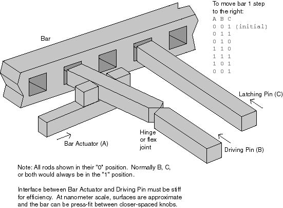
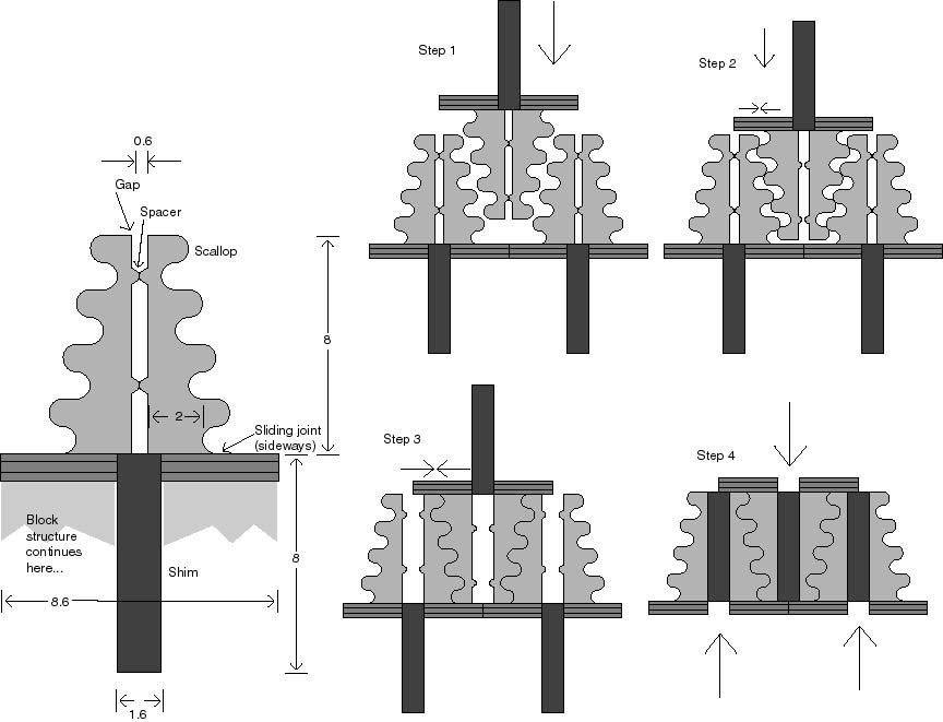
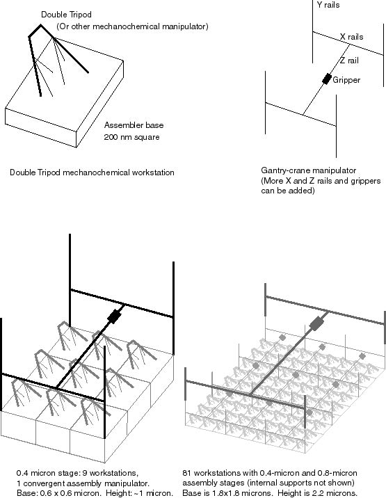
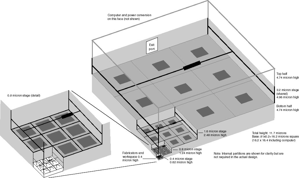
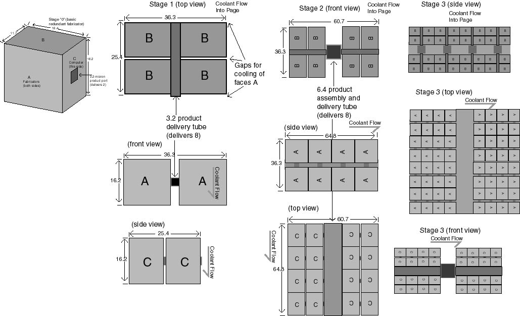
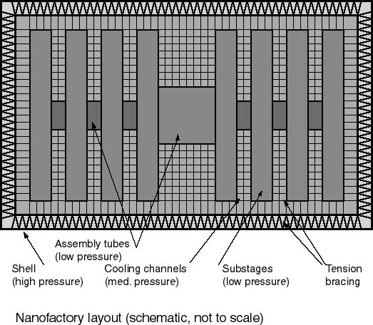